


Chapter 23 Memory Mapping Control (S12XMMCV2)
MC9S12XDP512 Data Sheet, Rev. 2.11
892 Freescale Semiconductor
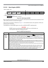
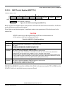
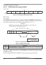
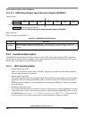
23.3.2.6 RAM Page Index Register (RPAGE)
Read: Anytime
Write: Anytime
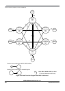
The RAM page index register allows accessing up to (1M minus 2K) bytes of RAM in the global memory
map by using the eight page index bits to page 4 Kbyte blocks into the RAM page window located in the
CPU local memory map from address $1000 to address $1FFF (see Figure 1-12).
CAUTION
XGATE write access to this register during an CPU access which makes use
of this register could lead to unexpected results.
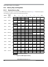
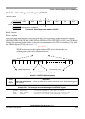
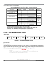
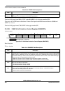
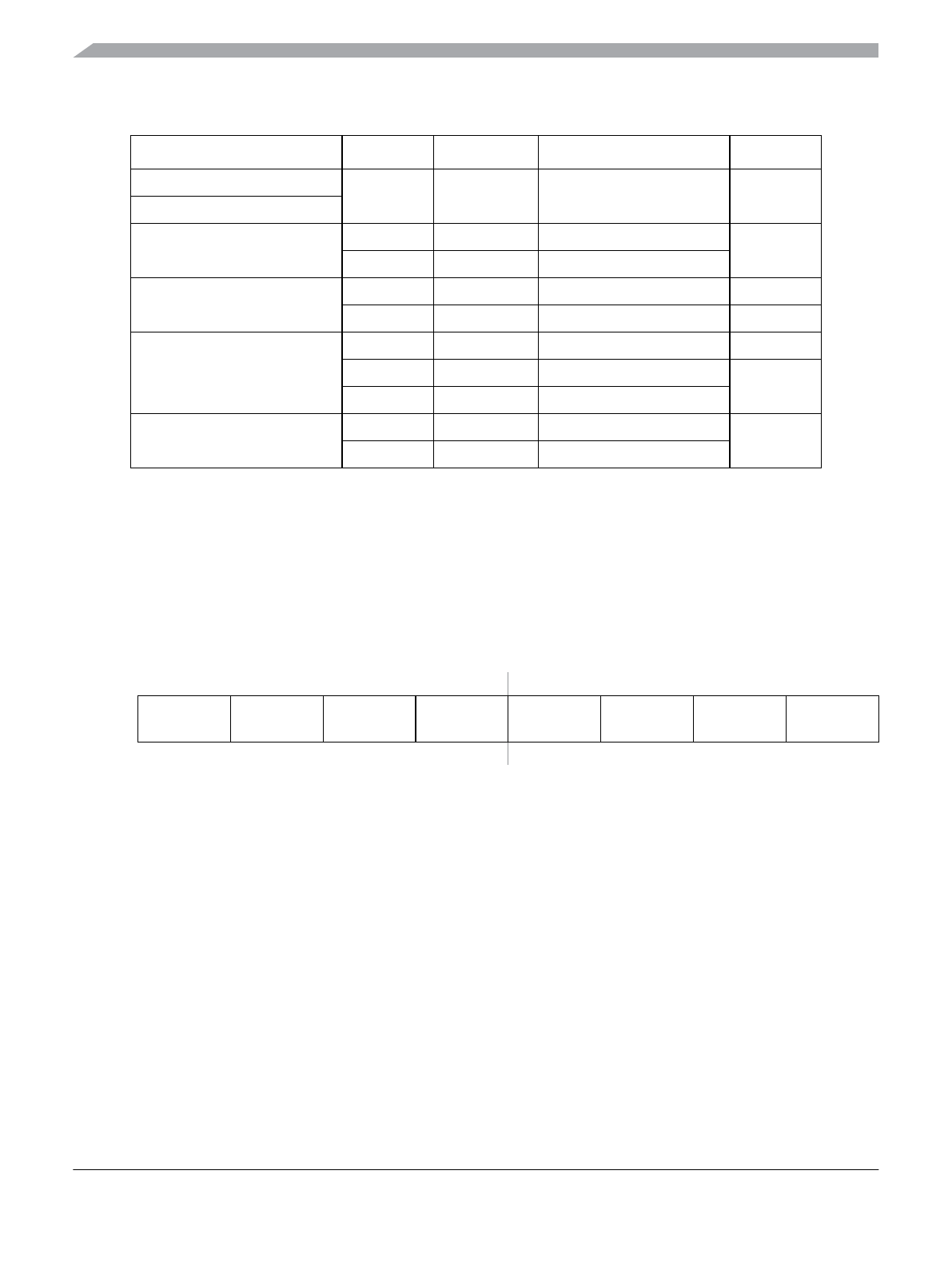
Table 23-10. Data Sources when CPU or BDM is Accessing Flash Area
Chip Modes ROMON EROMON DATA SOURCE
1
1
Internal means resources inside the MCU are read/written.
Internal Flash means Flash resources inside the MCU are read/written.
Emulation memory means resources inside the emulator are read/written (PRU registers, flash
replacement, RAM, EEPROM and register space are always considered internal).
External application means resources residing outside the MCU are read/written.
Stretch
2
2
The external access stretch mechanism is part of the EBI module (refer to EBI Block Guide for details).
Normal Single Chip X X Internal N
Special Single Chip
Emulation Single Chip X 0 Emulation Memory N
X 1 Internal Flash
Normal Expanded 0 X External Application Y
1 X Internal Flash N
Emulation Expanded 0 X External Application Y
1 0 Emulation Memory N
1 1 Internal Flash
Special Test 0 X External Application N
1 X Internal Flash
Address: 0x0016
76543210
R
RP7 RP6 RP5 RP4 RP3 RP2 RP1 RP0
W
Reset 11111101
Figure 23-11. RAM Page Index Register (RPAGE)