


Chapter 9 XGATE (S12XGATEV2)
MC9S12XDP512 Data Sheet, Rev. 2.11
402 Freescale Semiconductor
9.8.1.8 Dyadic Addressing (DYA)
In this mode the result of an operation between two registers is stored in one of the registers used as
operands.
RD = RD ∗ RS is the general register to register format, with register RD being the first operand and RS
the second. RD and RS can be any of the 8 general purpose registers R0 … R7. If R0 is used as the
destination register, only the condition code flags are updated. This addressing mode is used only for shift
operations with a variable shift value
Examples:
LSL R4,R5 ; R4 = R4 << R5
LSR R4,R5 ; R4 = R4 >> R5
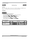
9.8.1.9 Triadic Addressing (TRI)
In this mode the result of an operation between two or three registers is stored into a third one.
RD = RS1 ∗ RS2 is the general format used in the order RD, RS1, RS1. RD, RS1, RS2 can be any of the
8 general purpose registers R0 … R7. If R0 is used as the destination register RD, only the condition code
flags are updated. This addressing mode is used for all arithmetic and logical operations.
Examples:
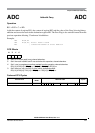
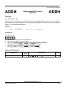
ADC R5,R6,R7 ; R5 = R6 + R7 + Carry
SUB R5,R6,R7 ; R5 = R6 - R7
9.8.1.10 Relative Addressing 9-Bit Wide (REL9)
A 9-bit signed word address offset is included in the instruction word. This addressing mode is used for
conditional branch instructions.
Examples:
BCC REL9 ; PC = PC + 2 + (REL9 << 1)
BEQ REL9 ; PC = PC + 2 + (REL9 << 1)
9.8.1.11 Relative Addressing 10-Bit Wide (REL10)
An 11-bit signed word address offset is included in the instruction word. This addressing mode is used for
the unconditional branch instruction.
Examples:
BRA REL10 ; PC = PC + 2 + (REL10 << 1)
9.8.1.12 Index Register plus Immediate Offset (IDO5)
(RS, #offset5) provides an unsigned offset from the base register.
Examples:
LDB R4,(R1,#offset) ; loads a byte from R1+offset into R4
STW R4,(R1,#offset) ; stores R4 as a word to R1+offset