


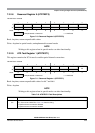
Chapter 7 Analog-to-Digital Converter (ATD10B16CV4)
MC9S12XDP512 Data Sheet, Rev. 2.11
Freescale Semiconductor 341
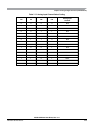
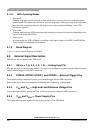
7.3.2.16 ATD Conversion Result Registers (ATDDRx)
The A/D conversion results are stored in 16 read-only result registers. The result data is formatted in the
result registers bases on two criteria. First there is left and right justification; this selection is made using
the DJM control bit in ATDCTL5. Second there is signed and unsigned data; this selection is made using
the DSGN control bit in ATDCTL5. Signed data is stored in 2’s complement format and only exists in left
justified format. Signed data selected for right justified format is ignored.
Read: Anytime
Write: Anytime in special mode, unimplemented in normal modes
7.3.2.16.1 Left Justified Result Data
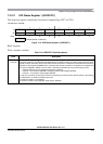
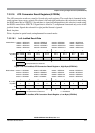
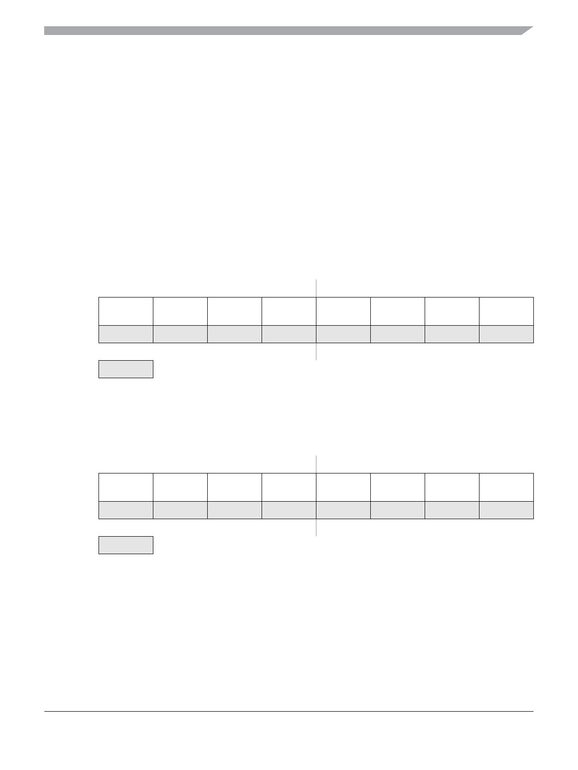
Module Base + 0x0010 = ATDDR0H
0x0012 = ATDDR1H
0x0014 = ATDDR2H
0x0016 = ATDDR3H
0x0018 = ATDDR4H
0x001A = ATDDR5H
0x001C = ATDDR6H
0x001E = ATDDR7H
0x0020 = ATDDR8H
0x0022 = ATDDR9H
0x0024 = ATDDR10H
0x0026 = ATDDR11H
0x0028 = ATDDR12H
0x002A = ATDDR13H
0x002C = ATDDR14H
0x002E = ATDDR15H
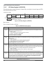
76543210
R (10-BIT)
R (8-BIT)
BIT 9 MSB
BIT 7 MSB
BIT 8
BIT 6
BIT 7
BIT 5
BIT 6
BIT 4
BIT 5
BIT 3
BIT 4
BIT 2
BIT 3
BIT 1
BIT 2
BIT 0
W
Reset 00000000
= Unimplemented or Reserved
Figure 7-18. Left Justified, ATD Conversion Result Register x, High Byte (ATDDRxH)
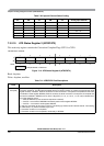
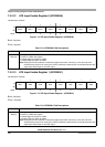
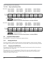
Module Base + 0x0011 = ATDDR0L
0x0013 = ATDDR1L
0x0015 = ATDDR2L
0x0017 = ATDDR3L
0x0019 = ATDDR4L
0x001B = ATDDR5L
0x001D = ATDDR6L
0x001F = ATDDR7L
0x0021 = ATDDR8L
0x0023 = ATDDR9L
0x0025 = ATDDR10L
0x0027 = ATDDR11L
0x0029 = ATDDR12L
0x002B = ATDDR13L
0x002D = ATDDR14L
0x002F = ATDDR15L
76543210
R (10-BIT)
R (8-BIT)
BIT 1
u
BIT 0
u
0
0
0
0
0
0
0
0
0
0
0
0
W
Reset 00000000
= Unimplemented or Reserved u = Unaffected
Figure 7-19. Left Justified, ATD Conversion Result Register x, Low Byte (ATDDRxL)