


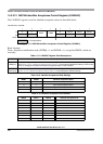

Chapter 14 Freescale’s Scalable Controller Area Network (S12MSCANV3)
MC9S12XDP512 Data Sheet, Rev. 2.11
644 Freescale Semiconductor
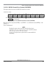
14.3.3 Programmer’s Model of Message Storage
The following section details the organization of the receive and transmit message buffers and the
associated control registers.
To simplify the programmer interface, the receive and transmit message buffers have the same outline.
Each message buffer allocates 16 bytes in the memory map containing a 13 byte data structure.
An additional transmit buffer priority register (TBPR) is defined for the transmit buffers. Within the last
two bytes of this memory map, the MSCAN stores a special 16-bit time stamp, which is sampled from an
internal timer after successful transmission or reception of a message. This feature is only available for
transmit and receiver buffers, if the TIME bit is set (see Section 14.3.2.1, “MSCAN Control Register 0
(CANCTL0)”).
The time stamp register is written by the MSCAN. The CPU can only read these registers.
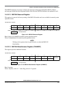
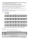
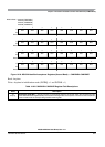
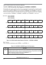
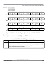
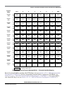
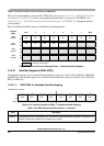
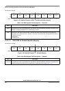
Figure 14-23 shows the common 13-byte data structure of receive and transmit buffers for extended
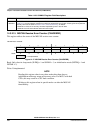
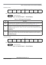
identifiers. The mapping of standard identifiers into the IDR registers is shown in Figure 14-24.
All bits of the receive and transmit buffers are ‘x’ out of reset because of RAM-based implementation
1
.
All reserved or unused bits of the receive and transmit buffers always read ‘x’.
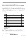
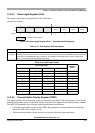
Table 14-25. Message Buffer Organization
Offset
Address
Register Access
0x00X0 Identifier Register 0
0x00X1 Identifier Register 1
0x00X2 Identifier Register 2
0x00X3 Identifier Register 3
0x00X4 Data Segment Register 0
0x00X5 Data Segment Register 1
0x00X6 Data Segment Register 2
0x00X7 Data Segment Register 3
0x00X8 Data Segment Register 4
0x00X9 Data Segment Register 5
0x00XA Data Segment Register 6
0x00XB Data Segment Register 7
0x00XC Data Length Register
0x00XD Transmit Buffer Priority Register
1
1
Not applicable for receive buffers
0x00XE Time Stamp Register (High Byte)
2
2
Read-only for CPU
0x00XF Time Stamp Register (Low Byte)
3
3
Read-only for CPU
1. Exception: The transmit priority registers are 0 out of reset.