


Chapter 8 Analog-to-Digital Converter (ATD10B8CV3)
MC9S12XDP512 Data Sheet, Rev. 2.11
348 Freescale Semiconductor
8.1.2.2 MCU Operating Modes
• Stop mode
Entering stop mode causes all clocks to halt and thus the system is placed in a minimum power
standby mode. This aborts any conversion sequence in progress. During recovery from stop mode,
there must be a minimum delay for the stop recovery time t
SR
before initiating a new ATD
conversion sequence.
• Wait mode
Entering wait mode the ATD conversion either continues or aborts for low power depending on the
logical value of the AWAIT bit.
• Freeze mode
In freeze mode the ATD will behave according to the logical values of the FRZ1 and FRZ0 bits.
This is useful for debugging and emulation.
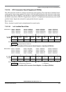
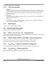
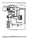
8.1.3 Block Diagram
Figure 8-1 shows a block diagram of the ATD.
8.2 External Signal Description
This section lists all inputs to the ATD block.
8.2.1 ANx (x = 7, 6, 5, 4, 3, 2, 1, 0) — Analog Input Pin
This pin serves as the analog input channel x. It can also be configured as general purpose digital port pin
and/or external trigger for the ATD conversion.
8.2.2 ETRIG3, ETRIG2, ETRIG1, and ETRIG0 — External Trigger Pins
These inputs can be configured to serve as an external trigger for the ATD conversion.
Refer to the device overview chapter for availability and connectivity of these inputs.
8.2.3 V
RH
and V
RL
— High and Low Reference Voltage Pins
V
RH
is the high reference voltage and V
RL
is the low reference voltage for ATD conversion.
8.2.4 V
DDA
and V
SSA
— Power Supply Pins
These pins are the power supplies for the analog circuitry of the ATD block.