


Appendix A Electrical Characteristics
MC9S12XDP512 Data Sheet, Rev. 2.11
Freescale Semiconductor 927
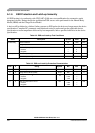
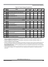
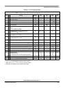
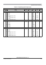
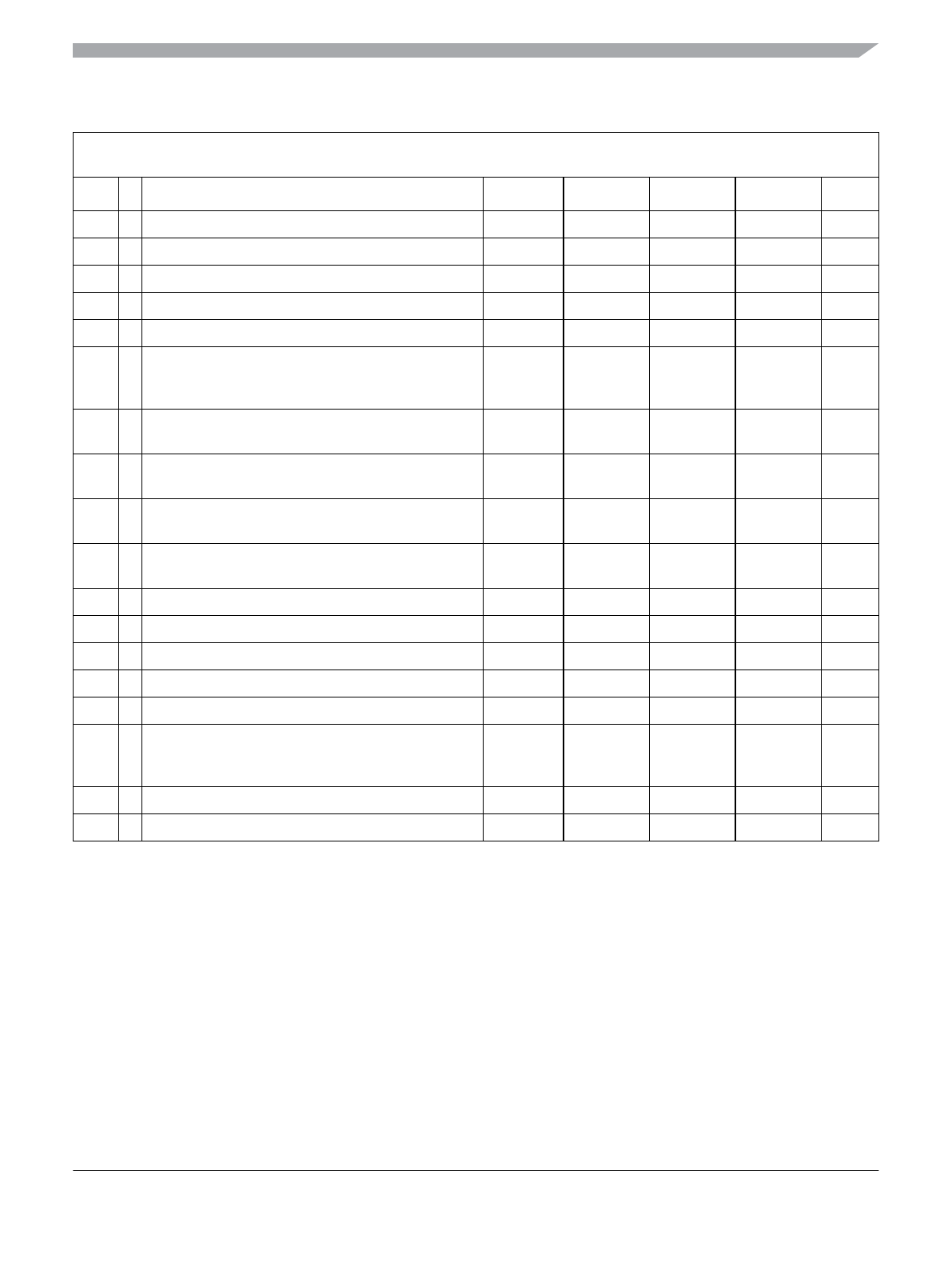
Table A-7. 5-V I/O Characteristics
Conditions are 4.5 V < V
DD35
< 5.5 V temperature from –40°C to +140°C, unless otherwise noted
I/O Characteristics for all I/O pins except EXTAL, XTAL,XFC,TEST and supply pins.
Num C Rating Symbol Min Typ Max Unit
1 P Input high voltage V
IH
0.65*V
DD35
——V
T Input high voltage V
IH
——V
DD35
+ 0.3 V
2 P Input low voltage V
IL
— — 0.35*V
DD35
V
T Input low voltage V
IL
V
SS35
– 0.3 — — V
3 C Input hysteresis V
HYS
250 — mV
4 P Input leakage current (pins in high impedance input
mode)
1
V
in
= V
DD35
or V
SS35
I
in
–1 — 1 µA
5 C Output high voltage (pins in output mode)
Partial drive I
OH
= –2 mA
V
OH
V
DD35
– 0.8 — — V
6 P Output high voltage (pins in output mode)
Full drive I
OH
= –10 mA
V
OH
V
DD35
– 0.8 — — V
7 C Output low voltage (pins in output mode)
Partial drive I
OL
= +2 mA
V
OL
— — 0.8 V
8 P Output low voltage (pins in output mode)
Full drive I
OL
= +10 mA
V
OL
— — 0.8 V
9 P Internal pull up device current, tested at V
IL
max I
PUL
— — –130 µA
10 C Internal pull up device current, tested at V
IH
min I
PUH
–10 — — µA
11 P Internal pull down device current, tested at V
IH
min I
PDH
— — 130 µA
12 C Internal pull down device current, tested at V
IL
max I
PDL
10 — — µA
13 D Input capacitance C
in
—6—pF
14 T Injection current
2
Single pin limit
Total device Limit, sum of all injected currents
I
ICS
I
ICP
–2.5
–25
—
2.5
25
mA
15 P Port H, J, P interrupt input pulse filtered
3
t
PULSE
—— 3µs
16 P Port H, J, P interrupt input pulse passed
3
t
PULSE
10 — — µs
1
Maximum leakage current occurs at maximum operating temperature. Current decreases by approximately one-half for each
8 C to 12 C in the temperature range from 50°C to 125°C.
2
Refer to Section A.1.4, “Current Injection” for more details
3
Parameter only applies in stop or pseudo stop mode.