


Chapter 6 Pierce Oscillator (S12XOSCLCPV1)
MC9S12XDP512 Data Sheet, Rev. 2.11
312 Freescale Semiconductor
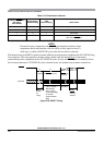
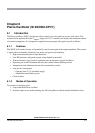
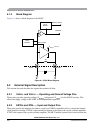
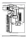
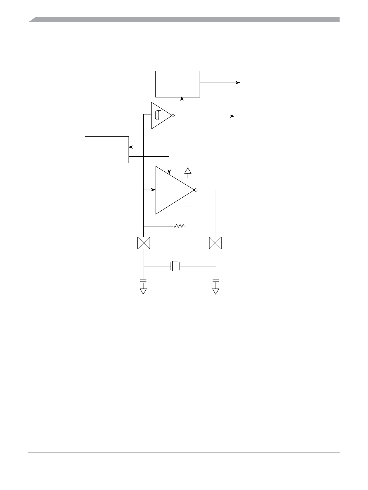
6.1.3 Block Diagram
Figure 6-1 shows a block diagram of the XOSC.
Figure 6-1. XOSC Block Diagram
6.2 External Signal Description
This section lists and describes the signals that connect off chip
6.2.1 V
DDPLL
and V
SSPLL
— Operating and Ground Voltage Pins
Theses pins provides operating voltage (V
DDPLL
) and ground (V
SSPLL
) for the XOSC circuitry. This
allows the supply voltage to the XOSC to be independently bypassed.
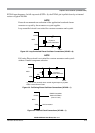
6.2.2 EXTAL and XTAL — Input and Output Pins
These pins provide the interface for either a crystal or a CMOS compatible clock to control the internal
clock generator circuitry. EXTAL is the external clock input or the input to the crystal oscillator amplifier.
XTAL is the output of the crystal oscillator amplifier. The MCU internal system clock is derived from the
EXTAL
XTAL
Gain Control
V
DDPLL
= 2.5 V
Rf
OSCCLK
Monitor_Failure
Clock
Monitor
Peak
Detector