


Chapter 14 Freescale’s Scalable Controller Area Network (S12MSCANV3)
MC9S12XDP512 Data Sheet, Rev. 2.11
640 Freescale Semiconductor
14.3.2.17 MSCAN Identifier Acceptance Registers (CANIDAR0-7)
On reception, each message is written into the background receive buffer. The CPU is only signalled to
read the message if it passes the criteria in the identifier acceptance and identifier mask registers
(accepted); otherwise, the message is overwritten by the next message (dropped).
The acceptance registers of the MSCAN are applied on the IDR0–IDR3 registers (see Section 14.3.3.1,
“Identifier Registers (IDR0–IDR3)”) of incoming messages in a bit by bit manner (see Section 14.4.3,
“Identifier Acceptance Filter”).
For extended identifiers, all four acceptance and mask registers are applied. For standard identifiers, only
the first two (CANIDAR0/1, CANIDMR0/1) are applied.
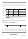
Read: Anytime
Write: Anytime in initialization mode (INITRQ = 1 and INITAK = 1)
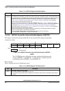
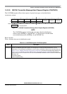
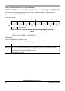
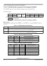
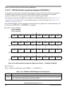
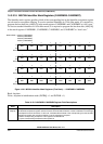
Module Base + 0x0010 (CANIDAR0)
0x0011 (CANIDAR1)
0x0012 (CANIDAR2)
0x0013 (CANIDAR3)
76543210
R
AC7 AC6 AC5 AC4 AC3 AC2 AC1 AC0
W
Reset 00000000
76543210
R
AC7 AC6 AC5 AC4 AC3 AC2 AC1 AC0
W
Reset 00000000
76543210
R
AC7 AC6 AC5 AC4 AC3 AC2 AC1 AC0
W
Reset 00000000
76543210
R
AC7 AC6 AC5 AC4 AC3 AC2 AC1 AC0
W
Reset 00000000
Figure 14-19. MSCAN Identifier Acceptance Registers (First Bank) — CANIDAR0–CANIDAR3
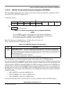
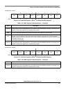
Table 14-21. CANIDAR0–CANIDAR3 Register Field Descriptions
Field Description
7:0
AC[7:0]
Acceptance Code Bits — AC[7:0] comprise a user-defined sequence of bits with which the corresponding bits
of the related identifier register (IDRn) of the receive message bufferare compared. The result of this comparison
is then masked with the corresponding identifier mask register.