


Chapter 7 Analog-to-Digital Converter (ATD10B16CV4)
MC9S12XDP512 Data Sheet, Rev. 2.11
332 Freescale Semiconductor
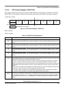
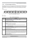
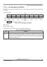
3:0
C[D:A}
Analog Input Channel Select Code — These bits select the analog input channel(s) whose signals are
sampled and converted to digital codes. Table 7-17 lists the coding used to select the various analog input
channels.
In the case of single channel conversions (MULT = 0), this selection code specified the channel to be examined.
In the case of multiple channel conversions (MULT = 1), this selection code represents the first channel to be
examined in the conversion sequence. Subsequent channels are determined by incrementing the channel
selection code or wrapping around to AN0 (after converting the channel defined by the Wrap Around Channel
Select Bits WRAP[3:0] in ATDCTL0). In case starting with a channel number higher than the one defined by
WRAP[3:0] the first wrap around will be AN15 to AN0.
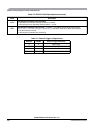
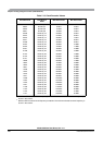
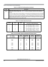
Table 7-15. Available Result Data Formats.
SRES8 DJM DSGN
Result Data Formats
Description and Bus Bit Mapping
1
1
1
0
0
0
0
0
1
0
0
1
0
1
X
0
1
X
8-bit / left justified / unsigned — bits 15:8
8-bit / left justified / signed — bits 15:8
8-bit / right justified / unsigned — bits 7:0
10-bit / left justified / unsigned — bits 15:6
10-bit / left justified / signed -— bits 15:6
10-bit / right justified / unsigned — bits 9:0
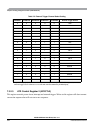
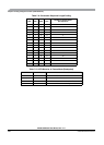
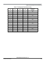
Table 7-16. Left Justified, Signed and Unsigned ATD Output Codes.
Input Signal
V
RL
= 0 Volts
V
RH
= 5.12 Volts
Signed
8-Bit Codes
Unsigned
8-Bit Codes
Signed
10-Bit Codes
Unsigned
10-Bit Codes
5.120 Volts
5.100
5.080
2.580
2.560
2.540
0.020
0.000
7F
7F
7E
01
00
FF
81
80
FF
FF
FE
81
80
7F
01
00
7FC0
7F00
7E00
0100
0000
FF00
8100
8000
FFC0
FF00
FE00
8100
8000
7F00
0100
0000
Table 7-14. ATDCTL5 Field Descriptions (continued)
Field Description