


Chapter 4 Port Integration Module (S12XDP512PIMV2)
MC9S12XDP512 Data Sheet, Rev. 2.11
Freescale Semiconductor 201
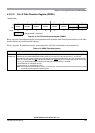
4.3.2.5 Port C Data Register (PORTC)
Read: Anytime. In emulation modes, read operations will return the data from the external bus, in all other
modes the data source is depending on the data direction value.
Write: Anytime. In emulation modes, write operations will also be directed to the external bus.
4.3.2.6 Port D Data Register (PORTD)
Read: Anytime. In emulation modes, read operations will return the data from the external bus, in all other
modes the data source is depending on the data direction value.
Write: Anytime. In emulation modes, write operations will also be directed to the external bus.
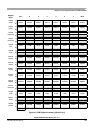
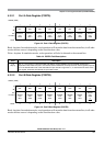
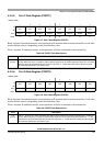
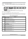
0x0004 (PRR)
76543210
R
PC7 PC6 PC5 PC4 PC3 PC2 PC1 PC0
W
Exp.: DATA15 DATA14 DATA13 DATA12 DATA11 DATA10 DATA9 DATA8
Reset 00000000
Figure 4-7. Port C Data Register (PORTC)
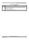
Table 4-8. PORTC Field Descriptions
Field Description
7–0
PC[7:0]
Port C — Port C pins 7–0 are associated with data I/O lines DATA15 through DATA8 respectively in expanded
modes. When this port is not used for external data, these pins can be used as general purpose I/O. If the data
direction bits of the associated I/O pins are set to logic level “1”, a read returns the value of the port register,
otherwise the buffered pin input state is read.
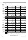
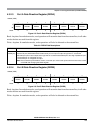
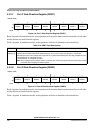
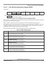
0x0005 (PRR)
76543210
R
PD7 PD6 PD5 PD4 PD3 PD2 PD1 PD0
W
Exp.: DATA7 DATA6 DATA5 DATA4 DATA3 DATA2 DATA1 DATA0
Reset 00000000
Figure 4-8. Port D Data Register (PORTD)
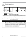
Table 4-9. PORTD Field Descriptions
Field Description
7–0
PD[7:0]
Port D — Port D pins 7–0 are associated with data I/O lines DATA7 through DATA0 respectively in expanded
modes. When this port is not used for external data, these pins can be used as general purpose I/O. — If the
data direction bits of the associated I/O pins are set to logic level “1”, a read returns the value of the port register,
otherwise the buffered pin input state is read.