


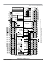
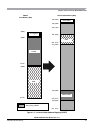
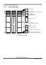
Chapter 1 Device Overview (MC9S12XDP512V2)
MC9S12XDP512 Data Sheet, Rev. 2.11
Freescale Semiconductor 35
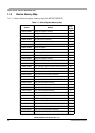
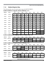
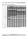
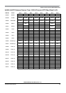
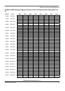
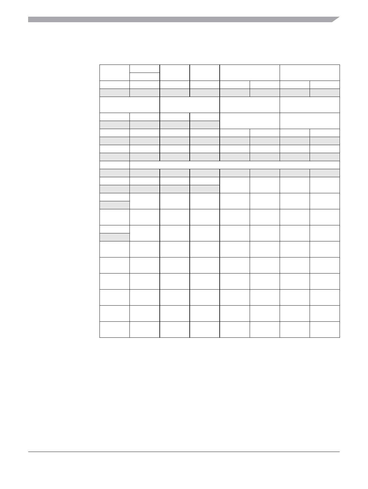
0x0020–0x0027 Debug Module (S12XDBG) Map
Address Name Bit 7 Bit 6 Bit 5 Bit 4 Bit 3 Bit 2 Bit 1 Bit 0
0x0020 DBGC1
R
ARM
0
XGSBPE BDM DBGBRK COMRV
W TRIG
0x0021 DBGSR
R TBF EXTF 0 0 0 SSF2 SSF1 SSF0
W
0x0022 DBGTCR
R
TSOURCE TRANGE TRCMOD TALIGN
W
0x0023 DBGC2
R0000
CDCM ABCM
W
0x0024 DBGTBH
R Bit 15 Bit 14 Bit 13 Bit 12 Bit 11 Bit 10 Bit 9 Bit 8
W
0x0025 DBGTBL
R Bit 7 Bit 6 Bit 5 Bit 4 Bit 3 Bit 2 Bit 1 Bit 0
W
0x0026 DBGCNT
R 0 CNT
W
0x0027 DBGSCRX
R0000
SC3 SC2 SC1 SC0
W
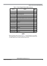
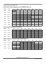
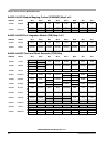
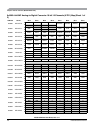
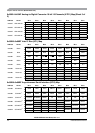
0x0028
1
1
This represents the contents if the Comparator A or C control register is blended into this address
DBGXCTL
(COMPA/C)
R0
NDB TAG BRK RW RWE SRC COMPE
W
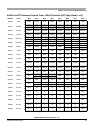
0x0028
2
2
This represents the contents if the Comparator B or D control register is blended into this address
DBGXCTL
(COMPB/D)
R
SZE SZ TAG BRK RW RWE SRC COMPE
W
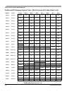
0x0029 DBGXAH
R0
Bit 22 21 20 19 18 17 Bit 16
W
0x002A DBGXAM
R
Bit 15 14 13 12 11 10 9 Bit 8
W
0x002B DBGXAL
R
Bit 7 6 54321Bit 0
W
0x002C DBGXDH
R
Bit 15 14 13 12 11 10 9 Bit 8
W
0x002D DBGXDL
R
Bit 7 654321Bit 0
W
0x002E DBGXDHM
R
Bit 15 14 13 12 11 10 9 Bit 8
W
0x002F DBGXDLM
R
Bit 7 654321Bit 0
W