


Chapter 17 Voltage Regulator (S12VREG3V3V5)
MC9S12XDP512 Data Sheet, Rev. 2.11
746 Freescale Semiconductor
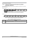
The API Trimming bits APITR[5:0] must be set so the minimum period equals 0.2 ms if stable frequency
is desired.
See Table 17-6 for the trimming effect of APITR.
NOTE
The first period after enabling the counter by APIFE might be reduced.
The API internal RC oscillator clock is not available if VREG_3V3 is in
Shutdown Mode.
17.4.8 Resets
This section describes how VREG_3V3 controls the reset of the MCU.The reset values of registers and
signals are provided in Section 17.3, “Memory Map and Register Definition”. Possible reset sources are
listed in Table 17-9.
17.4.9 Description of Reset Operation
17.4.9.1 Power-On Reset (POR)
During chip power-up the digital core may not work if its supply voltage V
DD
is below the POR
deassertion level (V
PORD
). Therefore, signal POR, which forces the other blocks of the device into reset,
is kept high until V
DD
exceeds V
PORD
. The MCU will run the start-up sequence after POR deassertion.
The power-on reset is active in all operation modes of VREG_3V3.
17.4.9.2 Low-Voltage Reset (LVR)
For details on low-voltage reset, see Section 17.4.5, “Low-Voltage Reset (LVR)”.
17.4.10 Interrupts
This section describes all interrupts originated by VREG_3V3.
The interrupt vectors requested by VREG_3V3 are listed in Table 17-10. Vector addresses and interrupt
priorities are defined at MCU level.
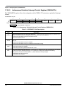
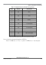
Table 17-9. Reset Sources
Reset Source Local Enable
Power-on reset Always active
Low-voltage reset Available only in Full Performance Mode
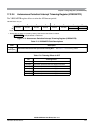
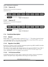
Table 17-10. Interrupt Vectors
Interrupt Source Local Enable
Low-voltage interrupt (LVI) LVIE = 1; available only in Full Performance
Mode