


Chapter 1 Device Overview (MC9S12XDP512V2)
MC9S12XDP512 Data Sheet, Rev. 2.11
Freescale Semiconductor 93
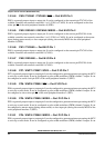
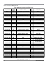
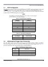
The configuration of the oscillator can be selected using the XCLKS signal (see Table 1-6). For a detailed
description please refer to the CRG Block Guide.
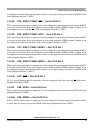
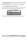
The logic level on the voltage regulator enable pin V
REGEN
determines whether the on-chip voltage
regulator is enabled or disabled (see Table 1-7).
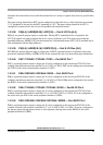
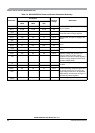
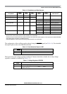
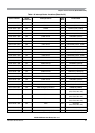
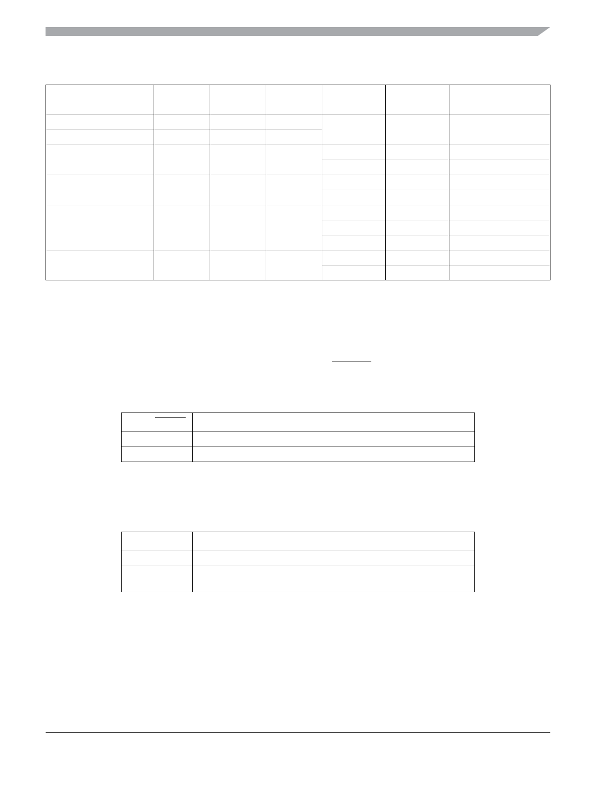
Table 1-5. Chip Modes and Data Sources
Chip Modes
BKGD =
MODC
PE6 =
MODB
PE5 =
MODA
PK7 =
ROMCTL
PE3 =
EROMCTL
Data Source
1
1
Internal means resources inside the MCU are read/written.
Internal Flash means Flash resources inside the MCU are read/written.
Emulation memory means resources inside the emulator are read/written (PRUregisters, Flash replacement, RAM, EEPROM,
and register space are always considered internal).
External application means resources residing outside the MCU are read/written.
Normal single chip 1 0 0 X X Internal
Special single chip 0 0 0
Emulation single chip 0 0 1 X 0 Emulation memory
X 1 Internal Flash
Normal expanded 1 0 1 0 X External application
1 X Internal Flash
Emulation expanded 0 1 1 0 X External application
1 0 Emulation memory
1 1 Internal Flash
Special test 0 1 0 0 X External application
1 X Internal Flash
Table 1-6. Clock Selection Based on PE7
PE7 = XCLKS Description
0 Full swing Pierce oscillator or external clock source selected
1 Loop controlled Pierce oscillator selected
Table 1-7. Voltage Regulator VREGEN
V
REGEN
Description
1 Internal voltage regulator enabled
0 Internal voltage regulator disabled, V
DD1,2
and V
DDPLL
must be
supplied externally