


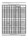
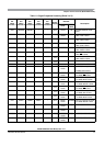

Chapter 1 Device Overview (MC9S12XDP512V2)
MC9S12XDP512 Data Sheet, Rev. 2.11
84 Freescale Semiconductor
1.2.3.30 PJ7 / KWJ7 / TXCAN4 / SCL0 / TXCAN0— PORT J I/O Pin 7
PJ7 is a general-purpose input or output pin. It can be configured to generate an interrupt causing the MCU
to exit stop or wait mode. It can be configured as the transmit pin TXCAN for the scalable controller area
network controller 0 or 4 (CAN0 or CAN4) or as the serial clock pin SCL of the IIC0 module.
1.2.3.31 PJ6 / KWJ6 / RXCAN4 / SDA0 / RXCAN0 — PORT J I/O Pin 6
PJ6 is a general-purpose input or output pin. It can be configured to generate an interrupt causing the MCU
to exit stop or wait mode. It can be configured as the receive pin RXCAN for the scalable controller area
network controller 0 or 4 (CAN0 or CAN4) or as the serial data pin SDA of the IIC0 module.
1.2.3.32 PJ5 / KWJ5 / SCL1 / CS2 — PORT J I/O Pin 5
PJ5 is a general-purpose input or output pin. It can be configured to generate an interrupt causing the MCU
to exit stop or wait mode. It can be configured as the serial clock pin SCL of the IIC1 module. It can be
configured to provide a chip-select output.
1.2.3.33 PJ4 / KWJ4 / SDA1 / CS0 — PORT J I/O Pin 4
PJ4 is a general-purpose input or output pin. It can be configured to generate an interrupt causing the MCU
to exit stop or wait mode. It can be configured as the serial data pin SDA of the IIC1 module. It can be
configured to provide a chip-select output.
1.2.3.34 PJ2 / KWJ2 / CS1 — PORT J I/O Pin 2
PJ2 is a general-purpose input or output pins. It can be configured to generate an interrupt causing the
MCU to exit stop or wait mode. It can be configured to provide a chip-select output.
1.2.3.35 PJ1 / KWJ1 / TXD2 — PORT J I/O Pin 1
PJ1 is a general-purpose input or output pin. It can be configured to generate an interrupt causing the MCU
to exit stop or wait mode. It can be configured as the transmit pin TXD of the serial communication
interface 2 (SCI2).
1.2.3.36 PJ0 / KWJ0 / RXD2 / CS3 — PORT J I/O Pin 0
PJ0 is a general-purpose input or output pin. It can be configured to generate an interrupt causing the MCU
to exit stop or wait mode. It can be configured as the receive pin RXD of theserial communication interface
2 (SCI2).It can be configured to provide a chip-select output.
1.2.3.37 PK7 / EWAIT / ROMCTL — Port K I/O Pin 7
PK7 is a general-purpose input or output pin. During MCU emulation modes and normal expanded modes
of operation, this pin is used to enable the Flash EEPROM memory in the memory map (ROMCTL). At
the rising edge of
RESET, the state of this pin is latched to the ROMON bit. The EWAIT input signal