


Chapter 11 Enhanced Capture Timer (S12MC9S12XDP51216B8CV2)
MC9S12XDP512 Data Sheet, Rev. 2.11
526 Freescale Semiconductor
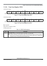
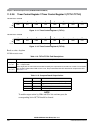
11.3.2.12 Main Timer Interrupt Flag 1 (TFLG1)
Read: Anytime
Write used in the flag clearing mechanism. Writing a one to the flag clears the flag. Writing a zero will not
affect the current status of the bit.
NOTE
When TFFCA = 1, the flags cannot be cleared via the normal flag clearing
mechanism (writing a one to the flag). Reference Section 11.3.2.6, “Timer
System Control Register 1 (TSCR1)”.
All bits reset to zero.
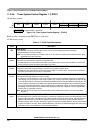
TFLG1 indicates when interrupt conditions have occurred. The flags can be cleared via the normal flag
clearing mechanism (writing a one to the flag) or via the fast flag clearing mechanism (reference TFFCA
bit in Section 11.3.2.6, “Timer System Control Register 1 (TSCR1)”).
Use of the TFMOD bit in the ICSYS register in conjunction with the use of the ICOVW register allows a
timer interrupt to be generated after capturing two values in the capture and holding registers, instead of
generating an interrupt for every capture.
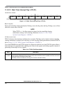
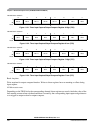
Module Base + 0x000E
76543210
R
C7F C6F C5F C4F C3F C2F C1F C0F
W
Reset 00000000
Figure 11-17. Main Timer Interrupt Flag 1 (TFLG1)
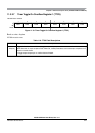
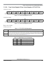
Table 11-16. TFLG1 Field Descriptions
Field Description
7:0
C[7:0]F
Input Capture/Output Compare Channel “x” Flag — A CxF flag is set when a corresponding input capture or
output compare is detected. C0F can also be set by 16-bit Pulse Accumulator B (PACB). C3F–C0F can also be
set by 8-bit pulse accumulators PAC3–PAC0.
If the delay counter is enabled, the CxF flag will not be set until after the delay.