


Chapter 7 Analog-to-Digital Converter (ATD10B16CV4)
MC9S12XDP512 Data Sheet, Rev. 2.11
Freescale Semiconductor 331
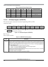
7.3.2.6 ATD Control Register 5 (ATDCTL5)
This register selects the type of conversion sequence and the analog input channels sampled. Writes to this
register will abort current conversion sequence and start a new conversion sequence. If external trigger is
enabled (ETRIGE = 1) an initial write to ATDCTL5 is required to allow starting of a conversion sequence
which will then occur on each trigger event. Start of conversion means the beginning of the sampling
phase.
Read: Anytime
Write: Anytime
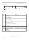
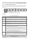
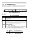
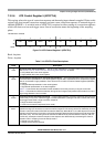
Module Base + 0x0005
76543210
R
DJM DSGN SCAN MULT CD CC CB CA
W
Reset 00000000
Figure 7-8. ATD Control Register 5 (ATDCTL5)
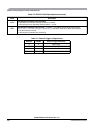
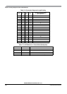
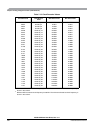
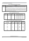
Table 7-14. ATDCTL5 Field Descriptions
Field Description
7
DJM
Result Register Data Justification — This bit controls justification of conversion data in the result registers.
See Section 7.3.2.16, “ATD Conversion Result Registers (ATDDRx)” for details.
0 Left justified data in the result registers.
1 Right justified data in the result registers.
6
DSGN
Result Register Data Signed or Unsigned Representation — This bit selects between signed and unsigned
conversion data representation in the result registers. Signed data is represented as 2’s complement. Signed
data is not available in right justification. See <st-bold>7.3.2.16 ATD Conversion Result Registers (ATDDRx)
for details.
0 Unsigned data representation in the result registers.
1 Signed data representation in the result registers.
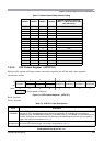
Table 7-15 summarizes the result data formats available and how they are set up using the control bits.
Table 7-16 illustrates the difference between the signed and unsigned, left justified output codes for an input
signal range between 0 and 5.12 Volts.
5
SCAN
Continuous Conversion Sequence Mode — This bit selects whether conversion sequences are performed
continuously or only once. If external trigger is enabled (ETRIGE=1) setting this bit has no effect, that means
each trigger event starts a single conversion sequence.
0 Single conversion sequence
1 Continuous conversion sequences (scan mode)
4
MULT
Multi-Channel Sample Mode — When MULT is 0, the ATD sequence controller samples only from the
specified analog input channel for an entire conversion sequence. The analog channel is selected by channel
selection code (control bits CD/CC/CB/CA located in ATDCTL5).When MULTis 1, the ATDsequence controller
samples across channels. The number of channels sampled is determined by the sequence length value(S8C,
S4C, S2C, S1C). The first analog channel examined is determined by channel selection code (CC, CB, CA
control bits); subsequent channels sampled in the sequence are determined by incrementing the channel
selection code or wrapping around to AN0 (channel 0.
0 Sample only one channel
1 Sample across several channels