


512 Kbyte Flash Module (S12XFTX512K4V2)
BookTitle, Rev. 2.4
110 Freescale Semiconductor
2.3.2.3 Flash Test Mode Register (FTSTMOD)
The FTSTMOD register is used to control Flash test features.
MRDS bits are readable and writable while all remaining bits read 0 and are not writable in normal mode.
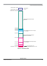
The WRALL bit is writable only in special mode to simplify mass erase and erase verify operations. When
writing to the FTSTMOD register in special mode, all unimplemented/reserved bits must be written to 0.
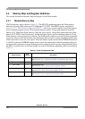
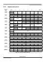
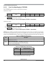
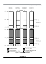
Module Base + 0x0002
76543210
R0
MRDS
00000
W
Reset 00000000
= Unimplemented or Reserved
Figure 2-6. Flash Test Mode Register (FTSTMOD —Normal Mode)
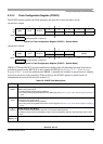
Module Base + 0x0002
76543210
R0
MRDS WRALL
0000
W
Reset 00000000
= Unimplemented or Reserved
Figure 2-7. Flash Test Mode Register (FTSTMOD — Special Mode)
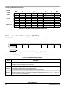
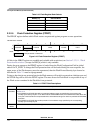
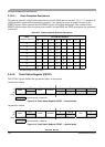
Table 2-7. FTSTMOD Field Descriptions
Field Description
6–5
MRDS[1:0]
Margin Read Setting — The MRDS[1:0] bits are used to set the sense-amp margin level for reads of the Flash
array as shown in Table 2-8.
4
WRALL
Write to all Register Banks — If the WRALL bit is set, all banked FDATA registers sharing the same register
address will be written simultaneously during a register write.
0 Write only to the FDATA register bank selected using BKSEL.
1 Write to all FDATA register banks.
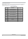
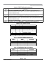
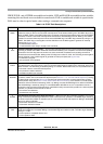
Table 2-8. FTSTMOD Margin Read Settings
MRDS[1:0] Margin Read Setting
00 Normal
01 Program Margin
1
1 Flash array reads will be sensitive to program margin.
10 Erase Margin
2
2 Flash array reads will be sensitive to erase margin.
11 Normal