


512 Kbyte Flash Module (S12XFTX512K4V2)
BookTitle, Rev. 2.4
122 Freescale Semiconductor
2.4 Functional Description
2.4.1 Flash Command Operations
Write operations are used to execute program, erase, erase verify, erase abort, and data compress
algorithms described in this section. The program and erase algorithms are controlled by a state machine
whose timebase, FCLK, is derived from the oscillator clock via a programmable divider. The command
register, as well as the associated address and data registers, operate as a buffer and a register (2-stage
FIFO) so that a second command along with the necessary data and address can be stored to the buffer
while the first command is still in progress. This pipelined operation allows a time optimization when
programming more than one word on a specific row in the Flash block as the high voltage generation can
be kept active in between two programming commands. The pipelined operation also allows a
simplification of command launching. Buffer empty as well as command completion are signalled by flags
in the Flash status register with corresponding interrupts generated, if enabled.
The next sections describe:
1. How to write the FCLKDIV register
2. Command write sequences to program, erase, erase verify, erase abort, and data compress
operations on the Flash memory
3. Valid Flash commands
4. Effects resulting from illegal Flash command write sequences or aborting Flash operations
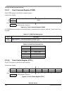
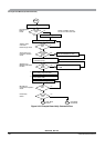
2.4.1.1 Writing the FCLKDIV Register
Prior to issuing any Flash command after a reset, the user is required to write the FCLKDIV register to
divide the oscillator clock down to within the 150 kHz to 200 kHz range. Since the program and erase
timings are also a function of the bus clock, the FCLKDIV determination must take this information into
account.
If we define:
• FCLK as the clock of the Flash timing control block
• Tbus as the period of the bus clock
• INT(x) as taking the integer part of x (e.g. INT(4.323) = 4)
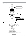
then FCLKDIV register bits PRDIV8 and FDIV[5:0] are to be set as described in Figure 2-24.
For example, if the oscillator clock frequency is 950kHz and the bus clock frequency is 10MHz,
FCLKDIV bits FDIV[5:0] should be set to 0x04 (000100) and bit PRDIV8 set to 0. The resulting FCLK
frequency is then 190kHz. As a result, the Flash program and erase algorithm timings are increased over
the optimum target by:
If the oscillator clock frequency is 16MHz and the bus clock frequency is 40MHz, FCLKDIV bits
FDIV[5:0] should be set to 0x0A (001010) and bit PRDIV8 set to 1. The resulting FCLK frequency is then
200 190–()200⁄ 100× 5%=