


Chapter 13 Inter-Integrated Circuit (MC9S12XDP512) Block Description
MC9S12XDP512 Data Sheet, Rev. 2.11
Freescale Semiconductor 607
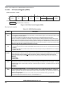
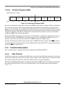
13.3.2.5 IIC Data I/O Register (IBDR)
In master transmit mode, when data is written to the IBDR a data transfer is initiated. The most significant
bit is sent first. In master receive mode, reading this register initiates next byte data receiving. In slave
mode, the same functions are available after an address match has occurred.Note that the Tx/Rx bit in the
IBCR must correctly reflect the desired direction of transfer in master and slave modes for the transmission
to begin. For instance, if the IIC is configured for master transmit but a master receive is desired, then
reading the IBDR will not initiate the receive.
Reading the IBDR will return the last byte received while the IIC is configured in either master receive or
slave receive modes. The IBDR does not reflect every byte that is transmitted on the IIC bus, nor can
software verify that a byte has been written to the IBDR correctly by reading it back.
In master transmit mode, the first byte of data written to IBDR following assertion of MS/
SL is used for
the address transfer and should com.prise of the calling address (in position D7:D1) concatenated with the
required R/
W bit (in position D0).
13.4 Functional Description
This section provides a complete functional description of the MC9S12XDP512.
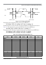
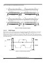
13.4.1 I-Bus Protocol
The IIC bus system uses a serial data line (SDA) and a serial clock line (SCL) for data transfer. All devices
connected to it must have open drain or open collector outputs. Logic AND function is exercised on both
lines with external pull-up resistors. The value of these resistors is system dependent.
Normally, a standard communication is composed of four parts: START signal, slave address transmission,
data transfer and STOP signal. They are described briefly in the following sections and illustrated in
Figure 13-9.
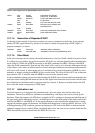
Offset Module Base + 0x0004
76543210
R
D7 D6 D5 D4 D3 D2 D1 D0
W
Reset 00000000
Figure 13-8. IIC Bus Data I/O Register (IBDR)