


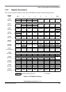
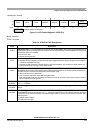

Chapter 7 Analog-to-Digital Converter (ATD10B16CV4)
MC9S12XDP512 Data Sheet, Rev. 2.11
Freescale Semiconductor 329
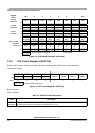
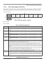
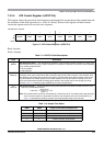
7.3.2.5 ATD Control Register 4 (ATDCTL4)
This register selects the conversion clock frequency, the length of the second phase of the sample time and
the resolution of the A/D conversion (i.e., 8-bits or 10-bits). Writes to this register will abort current
conversion sequence but will not start a new sequence.
Read: Anytime
Write: Anytime
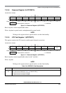
Module Base + 0x0004
76543210
R
SRES8 SMP1 SMP0 PRS4 PRS3 PRS2 PRS1 PRS0
W
Reset 00000101
Figure 7-7. ATD Control Register 4 (ATDCTL4)
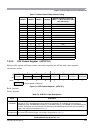
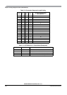
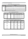
Table 7-11. ATDCTL4 Field Descriptions
Field Description
7
SRES8
A/D Resolution Select — This bit selects the resolution of A/D conversion results as either 8 or 10 bits. The
A/D converter has an accuracy of 10 bits. However, if low resolution is required, the conversion can be speeded
up by selecting 8-bit resolution.
0 10 bit resolution
1 8 bit resolution
6:5
SMP[1:0]
Sample Time Select —These two bits select the length of the second phase of the sample time in units of ATD
conversion clock cycles. Note that the ATD conversion clock period is itself a function of the prescaler value
(bits PRS4-0). The sample time consists of two phases. The first phase is two ATD conversion clock cycles
long and transfers the sample quickly (via the buffer amplifier) onto the A/D machine’s storage node. The
second phase attaches the external analog signal directly to the storage node for final charging and high
accuracy. Table 7-12 lists the lengths available for the second sample phase.
4:0
PRS[4:0]
ATD Clock Prescaler — These 5 bits are the binary value prescaler value PRS. The ATD conversion clock
frequency is calculated as follows:
Note: The maximum ATD conversion clock frequency is half the bus clock. The default (after reset) prescaler
value is 5 which results in a default ATD conversion clock frequency that is bus clock divided by 12.
Table 7-13 illustrates the divide-by operation and the appropriate range of the bus clock.
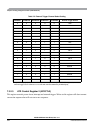
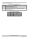
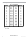
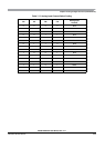
Table 7-12. Sample Time Select
SMP1 SMP0 Length of 2nd Phase of Sample Time
0 0 2 A/D conversion clock periods
0 1 4 A/D conversion clock periods
1 0 8 A/D conversion clock periods
1 1 16 A/D conversion clock periods
ATDclock
BusClock[]
PRS 1+[]
--------------------------------
0.5×=