


Chapter 7 Analog-to-Digital Converter (ATD10B16CV4)
MC9S12XDP512 Data Sheet, Rev. 2.11
Freescale Semiconductor 327
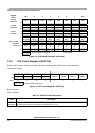
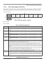
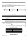
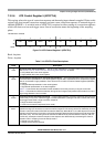
7.3.2.4 ATD Control Register 3 (ATDCTL3)
This register controls the conversion sequence length, FIFO for results registers and behavior in Freeze
Mode. Writes to this register will abort current conversion sequence but will not start a new sequence.
Read: Anytime
Write: Anytime
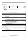
Module Base + 0x0003
76543210
R0
S8C S4C S2C S1C FIFO FRZ1 FRZ0
W
Reset 00100000
= Unimplemented or Reserved
Figure 7-6. ATD Control Register 3 (ATDCTL3)
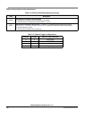
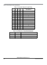
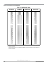
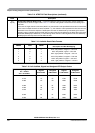
Table 7-8. ATDCTL3 Field Descriptions
Field Description
6
S8C
Conversion Sequence Length — This bit controls the number of conversions per sequence. Table 7-9 shows
all combinations. At reset, S4C is set to 1 (sequence length is 4). This is to maintain software continuity to HC12
Family.
5
S4C
Conversion Sequence Length — This bit controls the number of conversions per sequence. Table 7-9 shows
all combinations. At reset, S4C is set to 1 (sequence length is 4). This is to maintain software continuity to HC12
Family.
4
S2C
Conversion Sequence Length — This bit controls the number of conversions per sequence. Table 7-9 shows
all combinations. At reset, S4C is set to 1 (sequence length is 4). This is to maintain software continuity to HC12
Family.
3
S1C
Conversion Sequence Length — This bit controls the number of conversions per sequence. Table 7-9 shows
all combinations. At reset, S4C is set to 1 (sequence length is 4). This is to maintain software continuity to HC12
Family.
2
FIFO
Result Register FIFO Mode —If this bit is zero (non-FIFO mode), the A/D conversion results map into the
result registers based on the conversion sequence; the result of the first conversion appears in the first result
register, the second result in the second result register, and so on.
If this bit is one (FIFO mode) the conversion counter is not reset at the beginning or ending of a conversion
sequence; conversion results are placed in consecutive result registers between sequences. The result
register counter wraps around when it reaches the end of the result register file. The conversion counter value
in ATDSTAT0 can be used to determine where in the result register file, the current conversion result will be
placed.
Finally, which result registers hold valid data can be tracked using the conversion complete flags. Fastflag clear
mode may or may not be useful in a particular application to track valid data.
0 Conversion results are placed in the corresponding result register up to the selected sequence length.
1 Conversion results are placed in consecutive result registers (wrap around at end).
1:0
FRZ[1:0]
Background Debug Freeze Enable — When debugging an application, it is useful in many cases to have the
ATDpause when a breakpoint (FreezeMode) is encountered. These 2 bits determine how the ATD will respond
to a breakpoint as shown in Table 7-10. Leakage onto the storage node and comparator reference capacitors
may compromise the accuracy of an immediately frozen conversion depending on the length of the freeze
period.