


Chapter 4 Port Integration Module (S12XDP512PIMV2)
MC9S12XDP512 Data Sheet, Rev. 2.11
180 Freescale Semiconductor
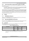
4.2 External Signal Description
This section lists and describes the signals that do connect off-chip.
4.2.1 Signal Properties
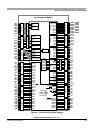
Table 4-1 shows all the pins and their functions that are controlled by the MC9S12XDP512. Refer to
Section 4.4, “Functional Description” for the availability of the individual pins in the different package
options.
NOTE
If there is more than one function associated with a pin, the priority is
indicated by the position in the table from top (highest priority) to bottom
(lowest priority).
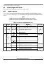
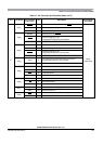
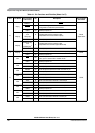
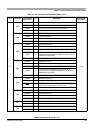
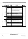
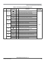
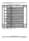
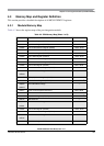
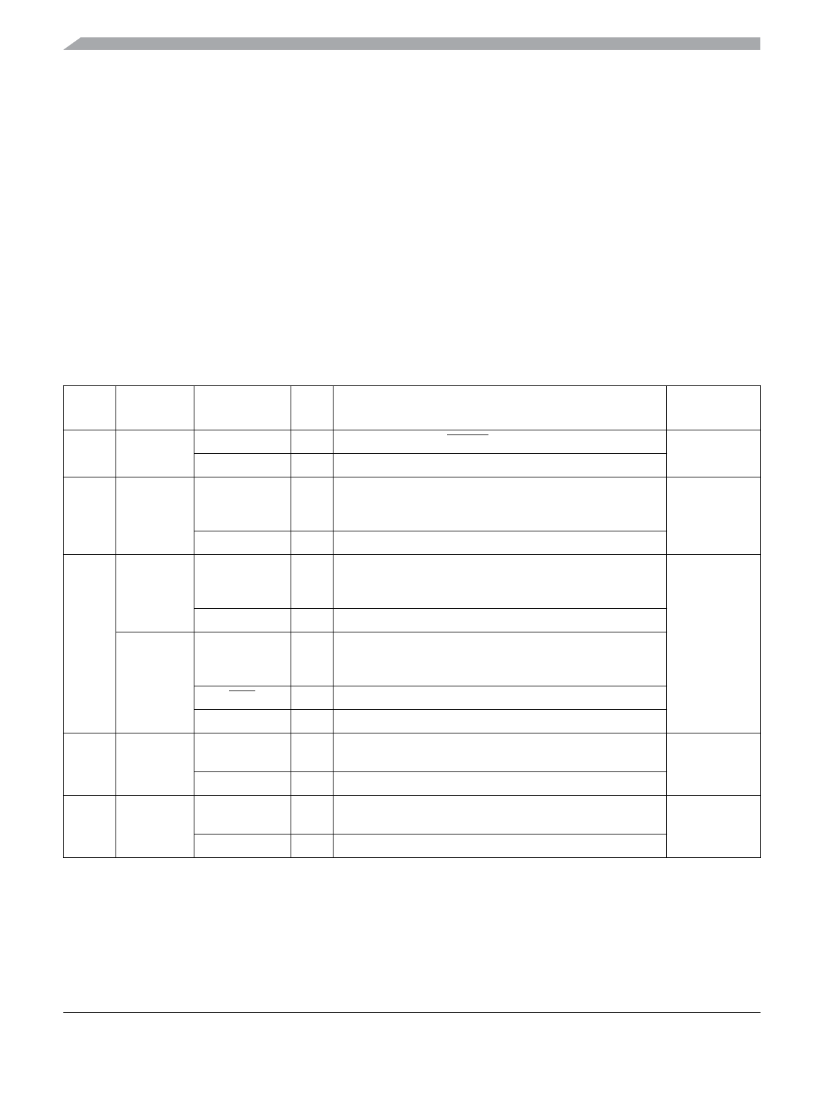
Table 4-1. Pin Functions and Priorities (Sheet 1 of 7)
Port Pin Name
Pin Function
and Priority
I/O Description
Pin Function
after Reset
— BKGD MODC
1
I MODC input during RESET BKGD
BKGD I/O S12X_BDM communication pin
A PA[7:0] ADDR[15:8]
mux
IVD[15:8]
2
O High-order external bus address output
(multiplexed with IVIS data)
Mode
dependent
3
GPIO I/O General-purpose I/O
B PB[7:1] ADDR[7:1]
mux
IVD[7:1]
2
O Low-order external bus address output
(multiplexed with IVIS data)
Mode
dependent
3
GPIO I/O General-purpose I/O
PB[0] ADDR[0]
mux
IVD0
2
O Low-order external bus address output
(multiplexed with IVIS data)
UDS O Upper data strobe
GPIO I/O General-purpose I/O
C PC[7:0] DATA[15:8] I/O High-order bidirectional data input/output
Configurable for reduced input threshold
Mode
dependent
3
GPIO I/O General-purpose I/O
D PD[7:0] DATA[7:0] I/O Low-order bidirectional data input/output
Configurable for reduced input threshold
Mode
dependent
3
GPIO I/O General-purpose I/O