


Chapter 17 Voltage Regulator (S12VREG3V3V5)
MC9S12XDP512 Data Sheet, Rev. 2.11
Freescale Semiconductor 737
17.2 External Signal Description
Due to the nature of VREG_3V3 being a voltage regulator providing the chip internal power supply
voltages, most signals are power supply signals connected to pads.
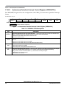
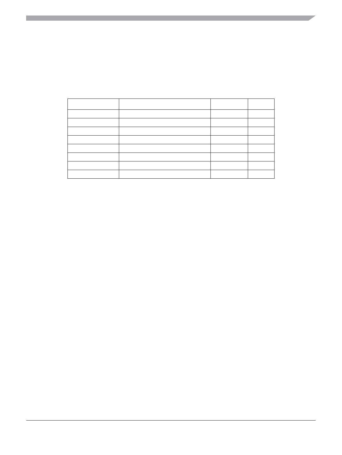
Table 17-1 shows all signals of VREG_3V3 associated with pins.
NOTE
Check device level specification for connectivity of the signals.
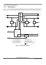
17.2.1 VDDR — Regulator Power Input Pins
Signal V
DDR
is the power input of VREG_3V3. All currents sourced into the regulator loads flow through
this pin. A chip external decoupling capacitor (100 nF...220 nF, X7R ceramic) between V
DDR
and V
SSR
(if V
SSR
is not available V
SS
) can smooth ripple on V
DDR
.
For entering Shutdown Mode, pin V
DDR
should also be tied to ground on devices without VREGEN pin.
17.2.2 VDDA, VSSA — Regulator Reference Supply Pins
Signals V
DDA
/V
SSA,
which are supposed to be relatively quiet, are used to supply the analog parts of the
regulator. Internal precision reference circuits are supplied from these signals. A chip external decoupling
capacitor (100 nF...220 nF, X7R ceramic) between V
DDA
and V
SSA
can further improve the quality of this
supply.
17.2.3 VDD, VSS — Regulator Output1 (Core Logic) Pins
Signals V
DD
/V
SS
are the primary outputs of VREG_3V3 that provide the power supply for the core logic.
These signals are connected to device pins to allow external decoupling capacitors (100 nF...220 nF, X7R
ceramic).
In Shutdown Mode an external supply driving V
DD
/V
SS
can replace the voltage regulator.
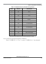
Table 17-1. Signal Properties
Name Function Reset State Pull Up
V
DDR
Power input (positive supply) — —
V
DDA
Quiet input (positive supply) — —
V
SSA
Quiet input (ground) — —
V
DD
Primary output (positive supply) — —
V
SS
Primary output (ground) — —
V
DDPLL
Secondary output (positive supply) — —
V
SSPLL
Secondary output (ground) — —
V
REGEN
(optional) Optional Regulator Enable — —