


Chapter 19 Background Debug Module (S12XBDMV2)
MC9S12XDP512 Data Sheet, Rev. 2.11
Freescale Semiconductor 779
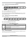
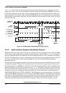
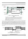
The external host should wait at least for 76 bus clock cycles after a TRACE1 or GO command before
starting any new serial command. This is to allow the CPU to exit gracefully from the standard BDM
firmware lookup table and resume execution of the user code. Disturbing the BDM shift register
prematurely may adversely affect the exit from the standard BDM firmware lookup table.
NOTE
If the bus rate of the target processor is unknown or could be changing or the
external wait function is used, it is recommended that the ACK
(acknowledge function) is used to indicate when an operation is complete.
When using ACK, the delay times are automated.
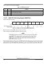
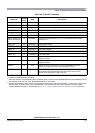
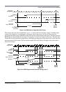
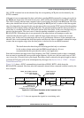
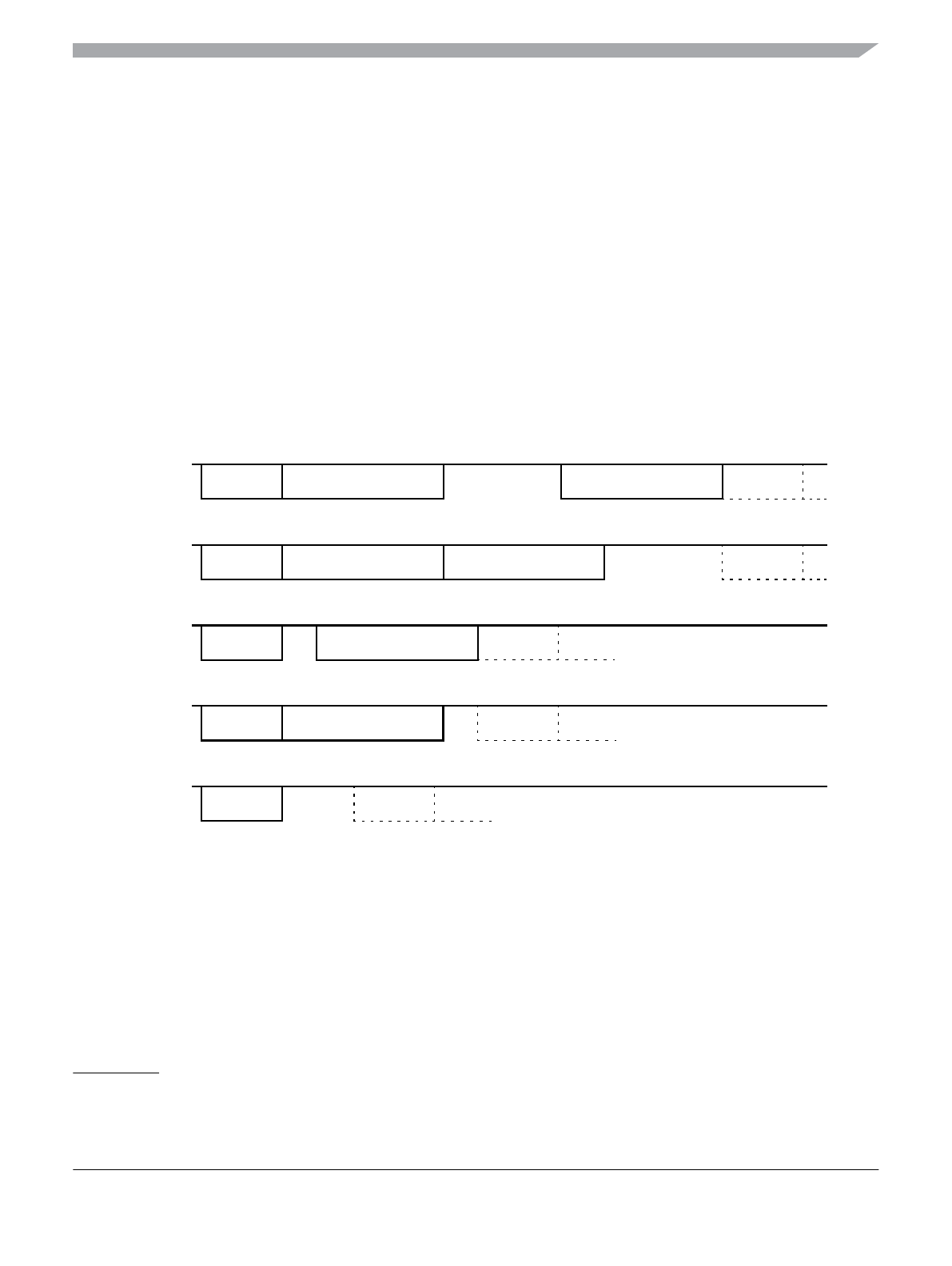
Figure 19-7 represents the BDM command structure. The command blocks illustrate a series of eight bit
times starting with a falling edge. The bar across the top of the blocks indicates that the BKGD line idles
in the high state. The time for an 8-bit command is 8 × 16 target clock cycles.
1
Figure 19-7. BDM Command Structure
1. Target clock cycles are cycles measured using the target MCU’s serial clock rate. See Section 19.4.6, “BDM Serial Interface”
and Section 19.3.2.1, “BDM Status Register (BDMSTS)” for information on how serial clock rate is selected.
Hardware
Hardware
Firmware
Firmware
GO,
48-BC
BC = Bus Clock Cycles
Command Address
150-BC
Delay
Next
DELAY
8 Bits
AT ~16 TC/Bit
16 Bits
AT ~16 TC/Bit
16 Bits
AT ~16 TC/Bit
Command Address Data
Next
Data
Read
Write
Read
Write
TRACE
Command
Next
Command Data
76-BC
Delay
Next
Command
150-BC
Delay
36-BC
DELAY
Command
Command
Command
Command
Data
Next
Command
TC = Target Clock Cycles