


Appendix A Electrical Characteristics
MC9S12XDP512 Data Sheet, Rev. 2.11
Freescale Semiconductor 933
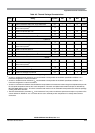
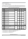
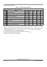
Table A-13. ATD Operating Characteristics 3.3V
A.2.2 Factors Influencing Accuracy
Three factors — source resistance, source capacitance and current injection — have an influence on the
accuracy of the ATD.
A.2.2.1 Source Resistance
Due to the input pin leakage current as specified in Table A-7 in conjunction with the source resistance
there will be a voltage drop from the signal source to the ATD input. The maximum source resistance R
S
specifies results in an error of less than 1/2 LSB (2.5 mV) at the maximum leakage current. If device or
operating conditions are less than worst case or leakage-induced error is acceptable, larger values of source
resistance is allowed.
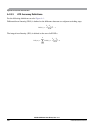
A.2.2.2 Source Capacitance
When sampling an additional internal capacitor is switched to the input. This can cause a voltage drop due
to charge sharing with the external and the pin capacitance. For a maximum sampling error of the input
voltage ≤ 1LSB, then the external filter capacitor, C
f
≥ 1024 * (C
INS
–C
INN
).
Conditions are shown in Table A-4 unless otherwise noted, Supply Voltage 3.15V < VDDA < 3.6V
Num C Rating Symbol Min Typ Max Unit
1 D Reference potential
Low
High
V
RL
V
RH
V
SSA
V
DDA
/2
—
—
V
DDA
/2
V
DDA
V
V
2 C Differential reference voltage
1
1
Full accuracy is not guaranteed when differential voltage is less than 3.15 V
V
RH
-V
RL
3.15 3.3 3.6 V
3 D ATD clock frequency f
ATDCLK
0.5 — 2.0 MHz
4 D ATD 10-bit conversion period
Clock cycles
2
Conv, time at 2.0 MHz ATD clock f
ATDCLK
2
The minimum time assumes a final sample period of 2 ATD clocks cycles while the maximum time assumes a final sample
period of 16 ATD clocks.
N
CONV10
T
CONV10
14
7
—
—
28
14
Cycles
µs
5 D ATD 8-bit conversion period
Clock cycles
2
Conv, time at 2.0 MHz ATD clock f
ATDCLK
N
CONV8
T
CONV8
12
6
—
—
26
13
Cycles
µs
6 D Recovery time (V
DDA
= 5.0 Volts) t
REC
——20µs
7 P Reference supply current 2 ATD blocks on I
REF
— — 0.500 mA
8 P Reference supply current 1 ATD block on I
REF
— — 0.250 mA