


Chapter 20 Debug (S12XDBGV2)
MC9S12XDP512 Data Sheet, Rev. 2.11
814 Freescale Semiconductor
If the TAG bit is clear (forced type trigger) a comparator match is generated when the selected address
appears on the system address bus. If the selected address is an opcode address, the match is generated
when the opcode is fetched from the memory. This precedes the instruction execution by an indefinite
number of cycles due to instruction pipe lining. For a comparator match of an opcode at an odd address
when TAG = 0, the corresponding even address must be contained in the comparator register. Thus for an
opcode at odd address (n), the comparator register must contain address (n – 1).
Once a successful comparator match has occurred, the condition that caused the original match is not
verified again on subsequent matches. Thus if a particular data value is verified at a given address, this
address may not still contain that data value when a subsequent match occurs.
Comparators C and D can also be used to select an address range to trace from. This is determined by the
TRANGE bits in the DBGTCR register. The TRANGE encoding is shown in Table 20-10. If the TRANGE
bits select a range definition using comparator D, then comparator D is configured for trace range
definition and cannot be used for address bus comparisons. Similarly if the TRANGE bits select a range
definition using comparator C, then comparator C is configured for trace range definition and cannot be
used for address bus comparisons.
Match[0,1,2,3] map directly to comparators [A,B,C,D] respectively, except in range modes (see
Section 20.3.1.4, “Debug Control Register2 (DBGC2)”). Comparator priority rules are described in the
trigger priority (see Section 20.4.3.6, “Trigger Priorities”).
20.4.2.1 Exact Address Comparator Match (Comparators A and C)
With range comparisons disabled, the match condition is an exact equivalence of address/data bus with the
value stored in the comparator address/data registers. Further qualification of the type of access (R/W,
word/byte) is possible.
Comparators A and C do not feature SZE or SZ control bits, thus the access size is not compared. The exact
address is compared, thus with the comparator address register loaded with address (n) a misaligned word
access of address (n-1) also accesses (n) but does not cause a match Table 20-37 lists access considerations
without data bus compare. Table 20-36 lists access considerations with data bus comparison. To compare
byte accesses DBGXDH must be loaded with the data byte. The low byte must be masked out using the
DBGXDLM mask register. On word accesses data byte of the lower address is mapped to DBGXDH.
Comparators A and C feature an NDB control bit to determine if a match occurs when the data bus differs
to comparator register contents or when the data bus is equivalent to the comparator register contents.
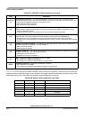
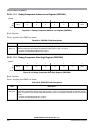
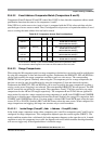
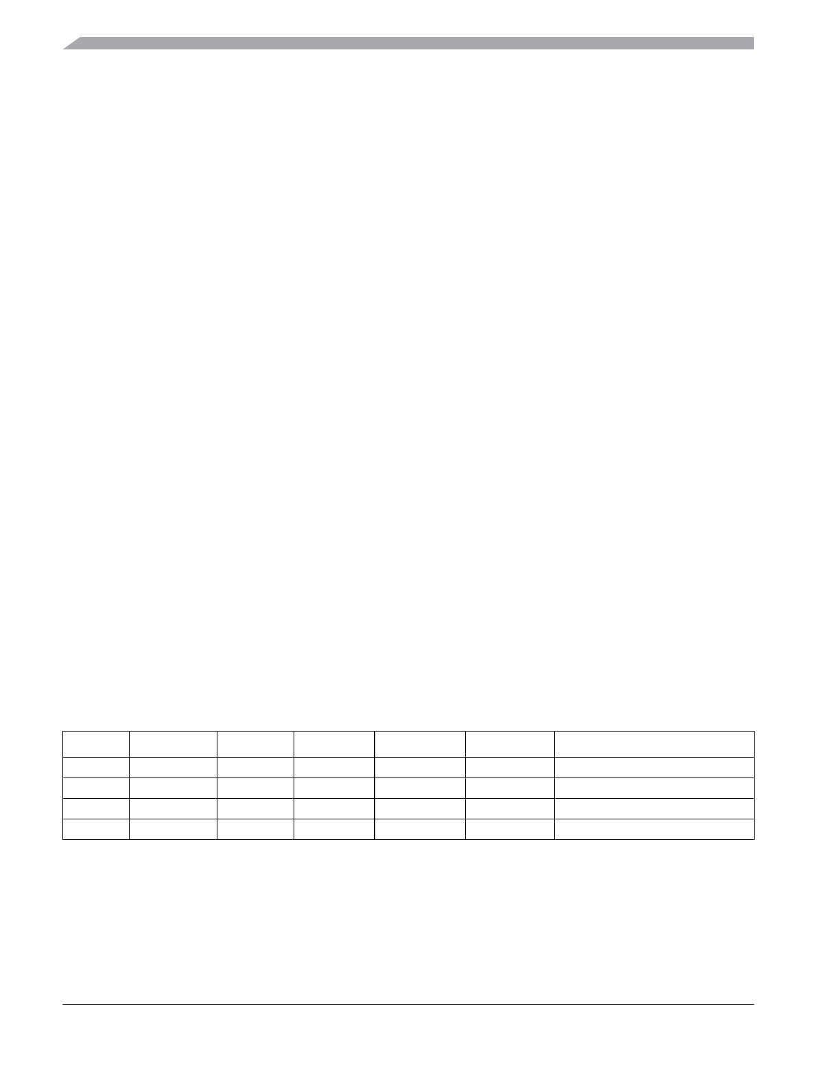
Table 20-36. Comparator A and C Data Bus Considerations
Access Address DBGxDH DBGxDL DBGxDHM DBGxDLM Example Valid Match
Word ADDR[n] Data[n] Data[n+1] 0x_FF 0x_FF MOVW #$WORD ADDR[n]
Byte ADDR[n] Data[n] x 0x_FF 0x_00 MOVB #$BYTE ADDR[n]
Word ADDR[n] Data[n] x 0x_FF 0x_00 MOVW #$WORD ADDR[n]
Word ADDR[n] x Data[n+1] 0x_00 0x_FF MOVW #$WORD ADDR[n]