


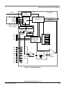

Chapter 7 Analog-to-Digital Converter (ATD10B16CV4)
MC9S12XDP512 Data Sheet, Rev. 2.11
344 Freescale Semiconductor
During a conversion, if additional active edges are detected the overrun error flag ETORF is set.
In either level or edge triggered modes, the first conversion begins when the trigger is received. In both
cases, the maximum latency time is one bus clock cycle plus any skew or delay introduced by the trigger
circuitry.
After ETRIGE is enabled, conversions cannot be started by a write to ATDCTL5, but rather must be
triggered externally.
If the level mode is active and the external trigger both de-asserts and re-asserts itself during a conversion
sequence, this does not constitute an overrun. Therefore, the flag is not set. If the trigger remains asserted
in level mode while a sequence is completing, another sequence will be triggered immediately.
7.4.2.2 General-Purpose Digital Input Port Operation
The input channel pins can be multiplexed between analog and digital data. As analog inputs, they are
multiplexed and sampled to supply signals to the A/D converter. As digital inputs, they supply external
input data that can be accessed through the digital port registers (PORTAD0 & PORTAD1) (input-only).
The analog/digital multiplex operation is performed in the input pads. The input pad is always connected
to the analog inputs of the ATD10B16C. The input pad signal is buffered to the digital port registers. This
buffer can be turned on or off with the ATDDIEN0 & ATDDIEN1 register. This is important so that the
buffer does not draw excess current when analog potentials are presented at its input.
7.4.3 Operation in Low Power Modes
The ATD10B16C can be configured for lower MCU power consumption in three different ways:
• Stop Mode
Stop Mode: This halts A/D conversion. Exit from Stop mode will resume A/D conversion, But due
to the recovery time the result of this conversion should be ignored.
Entering stop mode causes all clocks to halt and thus the system is placed in a minimum power
standby mode. This halts any conversion sequence in progress. During recovery from stop mode,
there must be a minimum delay for the stop recovery time t
SR
before initiating a new ATD
conversion sequence.
• Wait Mode
Wait Mode with AWAI = 1: This halts A/D conversion. Exit from Wait mode will resume A/D
conversion, but due to the recovery time the result of this conversion should be ignored.
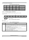
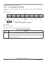
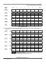
Table 7-27. External Trigger Control Bits
ETRIGLE ETRIGP ETRIGE SCAN Description
X X 0 0 Ignores external trigger. Performs one conversion sequence and stops.
X X 0 1 Ignores external trigger. Performs continuous conversion sequences.
0 0 1 X Falling edge triggered. Performs one conversion sequence per trigger.
0 1 1 X Rising edge triggered. Performs one conversion sequence per trigger.
1 0 1 X Trigger active low. Performs continuous conversions while trigger is active.
1 1 1 X Trigger active high. Performs continuous conversions while trigger is active.