


Appendix A Electrical Characteristics
MC9S12XDP512 Data Sheet, Rev. 2.11
958 Freescale Semiconductor
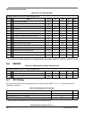
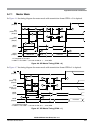
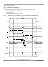
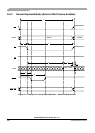
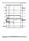
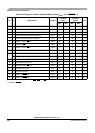
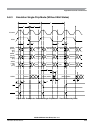
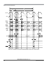
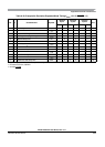
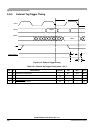
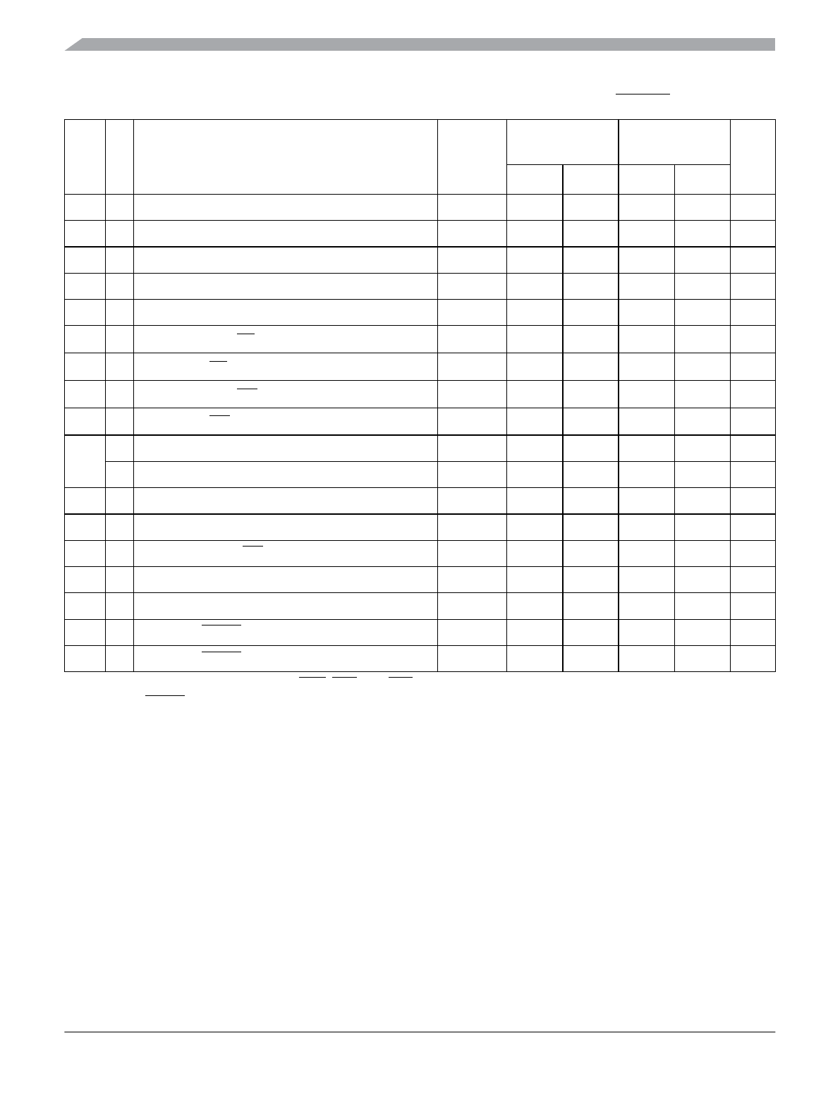
Table A-28. Example 1b: Normal Expanded Mode Timing V
DD35
= 5.0 V (EWAITE = 1)
No. C Characteristic Symbol
2 Stretch
Cycles
3 Stretch
Cycles
Unit
Min Max Min Max
— — Frequency of internal bus
f
i
D.C. 40.0 D.C. 40.0 MHz
— — Internal cycle time
t
cyc
25 ∞ 25 ∞ ns
— — Frequency of external bus
f
o
D.C. 13.3 D.C. 10.0 MHz
— — External cycle time (selected by EXSTR)
t
cyce
75 ∞ 100 ∞ ns
1 — External cycle time (EXSTR+1EWAIT)
t
cycew
100 ∞ 125 ∞ ns
2D
Address
1
valid to RE fall
1
Includes the following signals: ADDRx, UDS, LDS, and CSx.
t
ADRE
5—5—ns
3D
Pulse width,
RE
2
2
Affected by EWAIT.
PW
RE
85 — 110 — ns
4D
Address
1
valid to WE fall
t
ADWE
5—5—ns
5D
Pulse width,
WE
2
PW
WE
73 — 98 — ns
6
D Read data setup time (if ITHRS = 0)
t
DSR
24 — 24 — ns
D Read data setup time (if ITHRS = 1)
t
DSR
28 — 28 — ns
7 D Read data hold time
t
DHR
0—0—ns
8 D Read enable access time
t
ACCR
71 — 86 — ns
9 D Write data valid to
WE fall
t
WDWE
7—7—ns
10 D Write data setup time
t
DSW
81 — 106 — ns
11 D Write data hold time
t
DHW
8—8—ns
12 D Address to
EWAIT fall
t
ADWF
0 20 0 45 ns
13 D Address to
EWAIT rise
t
ADWR
37 47 62 72 ns