


Chapter 1 Device Overview (MC9S12XDP512V2)
MC9S12XDP512 Data Sheet, Rev. 2.11
Freescale Semiconductor 71
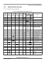
1.1.7 Part ID Assignments
The part ID is located in two 8-bit registers PARTIDH and PARTIDL (addresses 0x001A and 0x001B).
The read-only value is a unique part ID for each revision of the chip. Table 1-2 shows the assigned part ID
number and Mask Set number.
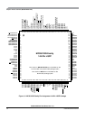
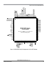
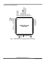
1.2 Signal Description
This section describes signals that connect off-chip. It includes a pinout diagram, a table of signal
properties, and detailed discussion of signals. It is built from the signal description sections of the Block
User Guides of the individual IP blocks on the device.
1.2.1 Device Pinout
The XD-Family of devices offers pin-compatible packaged devices to assist with system development and
accommodate expansion of the application.
The MC9S12XD-Family and MC9S12XA-Family devices are offered in the following package options:
• 144-pin LQFP package with an external bus interface (address/data bus)
• 112-pin LQFP without external bus interface
• 80-pin QFP without external bus interface
Most pins perform two or more functions, as described in more detail in Section 1.2.2, “Signal Properties
Summary”. Figure 1-5, Figure 1-6, and Figure 1-7 show the pin assignments for the various packages.
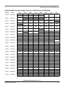
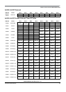
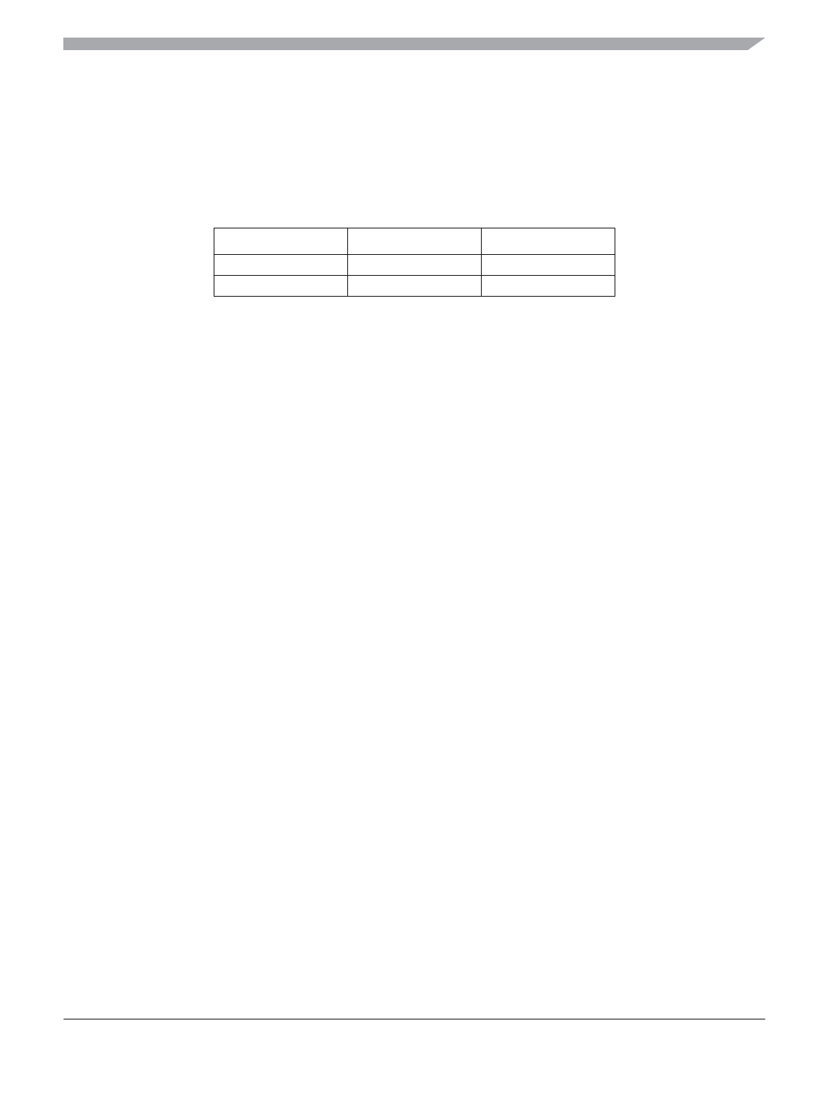
Table 1-2. Assigned Part ID Numbers
Device Mask Set Number Part ID
1
1
The coding is as follows:
Bit 15-12: Major family identifier
Bit 11-8: Minor family identifier
Bit 7-4: Major mask set revision number including FAB transfers
Bit 3-0: Minor — non full — mask set revision
MC9S12XDP512 L15Y 0xC410
MC9S12XDT384 L15Y 0xC410