


Chapter 8 Analog-to-Digital Converter (ATD10B8CV3)
MC9S12XDP512 Data Sheet, Rev. 2.11
350 Freescale Semiconductor
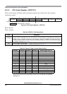
8.3 Memory Map and Register Definition
This section provides a detailed description of all registers accessible in the ATD.
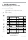
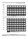
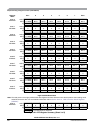
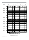
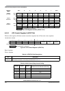
8.3.1 Module Memory Map
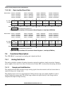
Figure 8-2 gives an overview of all ATD registers.
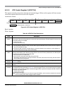
NOTE
Register Address = Base Address + Address Offset, where the Base Address
is defined at the MCU level and the Address Offset is defined at the module
level.
8.3.2 Register Descriptions
This section describes in address order all the ATD registers and their individual bits.
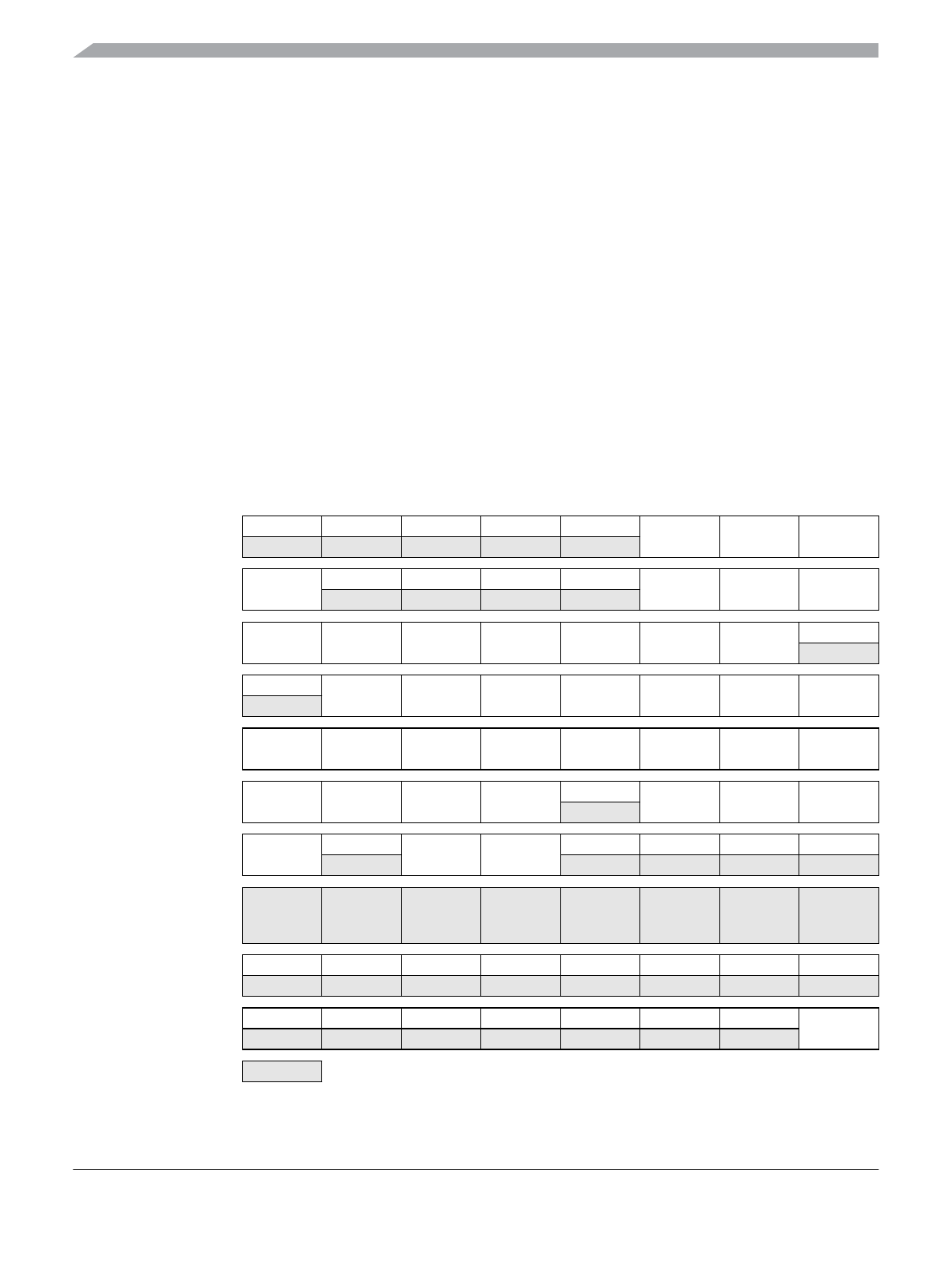
Register
Name
Bit 7 654321Bit 0
0x0000
ATDCTL0
R00000
WRAP2 WRAP1 WRAP0
W
0x0001
ATDCTL1
R
ETRIGSEL
0000
ETRIGCH2 ETRIGCH1 ETRIGCH0
W
0x0002
ATDCTL2
R
ADPU AFFC AWAI ETRIGLE ETRIGP ETRIGE ASCIE
ASCIF
W
0x0003
ATDCTL3
R0
S8C S4C S2C S1C FIFO FRZ1 FRZ0
W
0x0004
ATDCTL4
R
SRES8 SMP1 SMP0 PRS4 PRS3 PRS2 PRS1 PRS0
W
0x0005
ATDCTL5
R
DJM DSGN SCAN MULT
0
CC CB CA
W
0x0006
ATDSTAT0
R
SCF
0
ETORF FIFOR
0 CC2 CC1 CC0
W
0x0007
Unimplemente
d
R
W
0x0008
ATDTEST0
RUUUUUUUU
W
0x0009
ATDTEST1
RUU00000
SC
W
= Unimplemented or Reserved
Figure 8-2. ATD Register Summary (Sheet 1 of 5)