


Chapter 19 Background Debug Module (S12XBDMV2)
MC9S12XDP512 Data Sheet, Rev. 2.11
Freescale Semiconductor 781
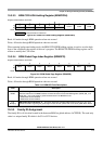
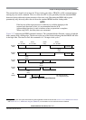
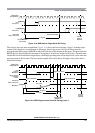
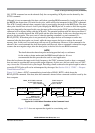
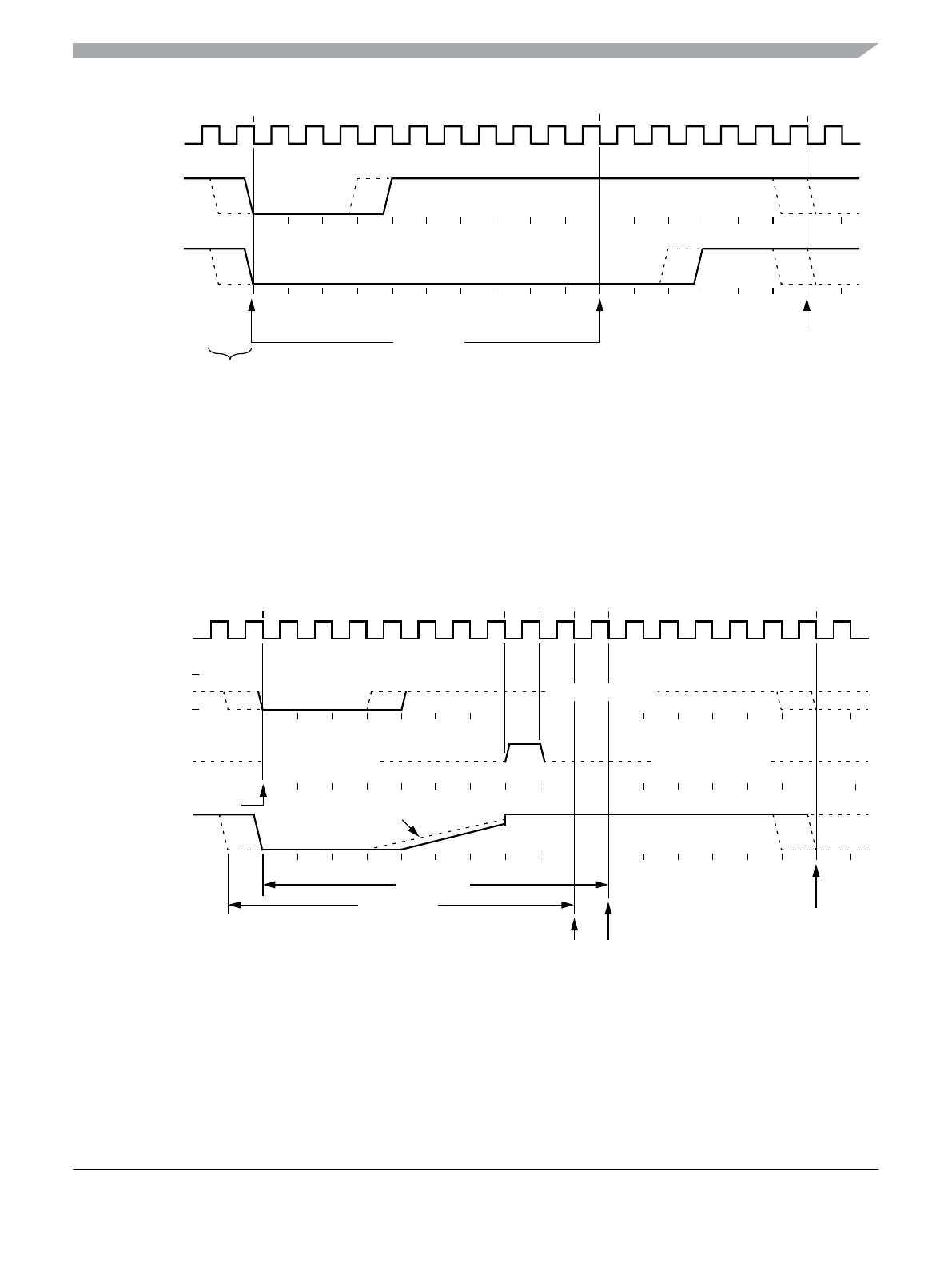
Figure 19-8. BDM Host-to-Target Serial Bit Timing
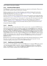
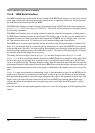
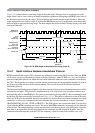
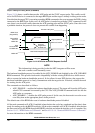
The receive cases are more complicated. Figure 19-9 shows the host receiving a logic 1 from the target
system. Since the host is asynchronous to the target, there is up to one clock-cycle delay from the
host-generated falling edge on BKGD to the perceived start of the bit time in the target. The host holds the
BKGD pin low long enough for the target to recognize it (at least two target clock cycles). The host must
release the low drive before the target drives a brief high speedup pulse seven target clock cycles after the
perceived start of the bit time. The host should sample the bit level about 10 target clock cycles after it
started the bit time.
Figure 19-9. BDM Target-to-Host Serial Bit Timing (Logic 1)
Target Senses Bit
10 Cycles
Synchronization
Uncertainty
BDM Clock
(Target MCU)
Host
Transmit 1
Host
Transmit 0
Perceived
Start of Bit Time
Earliest
Start of
Next Bit
High-Impedance
Earliest
Start of
Next Bit
R-C Rise
10 Cycles
10 Cycles
Host Samples
BKGD Pin
Perceived
Start of Bit Time
BKGD Pin
BDM Clock
(Target MCU)
Host
Drive to
BKGD Pin
Target System
Speedup
Pulse
High-Impedance
High-Impedance