


Chapter 4 Port Integration Module (S12XDP512PIMV2)
MC9S12XDP512 Data Sheet, Rev. 2.11
Freescale Semiconductor 197
4.3.2.1 Port A Data Register (PORTA)
Read: Anytime. In emulation modes, read operations will return the data from the external bus, in all other
modes the data source is depending on the data direction value.
Write: Anytime. In emulation modes, write operations will also be directed to the external bus.
4.3.2.2 Port B Data Register (PORTB)
Read: Anytime. In emulation modes, read operations will return the data from the external bus, in all other
modes the data source is depending on the data direction value.
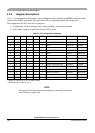
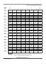
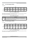
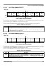
0x0000 (PRR)
76543210
R
PA7PA6PA5PA4PA3PA2PA1PA0
W
Alt.
Function
ADDR15
mux
IVD15
ADDR14
mux
IVD14
ADDR13
mux
IVD13
ADDR12
mux
IVD12
ADDR11
mux
IVD11
ADDR10
mux
IVD10
ADDR9
mux
IVD9
ADDR8
mux
IVD8
Reset 00000000
Figure 4-3. Port A Data Register (PORTA)
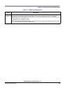
Table 4-4. PORTA Field Descriptions
Field Description
7–0
PA[7:0]
Port A — Port A pins 7–0 are associated with address outputs ADDR15 through ADDR8 respectively in
expanded modes. When this port is not used for external addresses, these pins can be used as general purpose
I/O. If the data direction bits of the associated I/O pins are set to logic level “1”, a read returns the value of the
port register, otherwise the buffered pin input state is read.
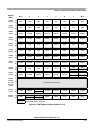
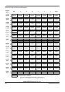
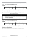
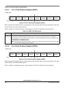
0x0001 (PRR)
76543210
R
PB7 PB6 PB5 PB4 PB3 PB2 PB1 PB0
W
Alt.
Function ADDR7
mux
IVD7
ADDR6
mux
IVD6
ADDR5
mux
IVD5
ADDR4
mux
IVD4
ADDR3
mux
IVD3
ADDR2
mux
IVD2
ADDR1
mux
IVD1
ADDR0
mux
IVD0
or
UDS
Reset 00000000
Figure 4-4. Port B Data Register (PORTB)