


Appendix A Electrical Characteristics
MC9S12XDP512 Data Sheet, Rev. 2.11
948 Freescale Semiconductor
And finally the frequency relationship is defined as
With the above values the resistance can be calculated. The example is shown for a loop bandwidth
f
C
= 20 kHz:
The capacitance C
s
can now be calculated as:
The capacitance C
p
should be chosen in the range of:
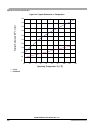
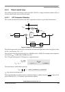
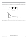
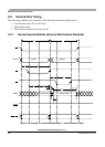
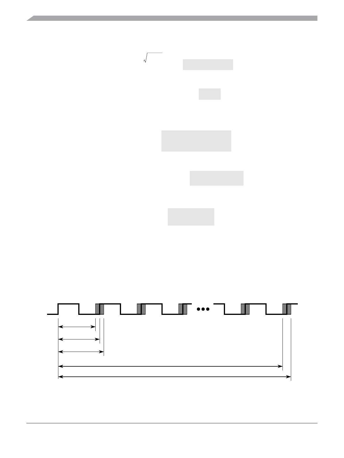
A.5.3.2 Jitter Information
The basic functionality of the PLL is shown in Figure A-3. With each transition of the clock f
cmp
, the
deviation from the reference clock f
ref
is measured and input voltage to the VCO is adjusted
accordingly.The adjustment is done continuously with no abrupt changes in the clock output frequency.
Noise, voltage, temperature and other factors cause slight variations in the control loop resulting in a clock
jitter. This jitter affects the real minimum and maximum clock periods as illustrated in Figure A-4.
Figure A-4. Jitter Definitions
f
C
2 ζ f
ref
⋅⋅
πζ 1 ζ
2
++
⎝⎠
⎛⎞
⋅
-------------------------------------------
1
10
-----
f
C
f
ref
410⋅
------------- ζ 0.9=();<→⋅<
f
C
< 100kHz
n
f
VCO
f
ref
--------------- 2 synr 1+()⋅==
= 20
R
2 π nf
C
⋅⋅⋅
K
Φ
-----------------------------
2 π 20 20kHz⋅⋅ ⋅
539.1Hz()Ω⁄
------------------------------------------
4.7kΩ===
C
s
2 ζ
2
⋅
π f
C
R⋅⋅
----------------------
0.516
f
C
R⋅
---------------
ζ 0.9=();==
= 5.5nF = ~ 4.7nF
C
s
20
------
C
p
C
s
10
------
≤≤
C
P
= 470pF
2 3 N-1 N1
0
t
nom
t
max1
t
min1
t
maxN
t
minN