


Chapter 20 Debug (S12XDBGV2)
MC9S12XDP512 Data Sheet, Rev. 2.11
812 Freescale Semiconductor
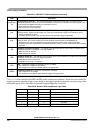
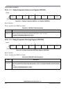
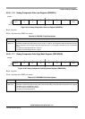
20.3.1.11.8 Debug Comparator Data Low Mask Register (DBGXDLM)
Read: Anytime
Write: Anytime when DBG not armed.
20.4 Functional Description
This section provides a complete functional description of the DBG module. If the part is in secure mode,
the DBG module can generate breakpoints but tracing is not possible.
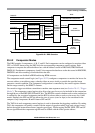
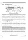
20.4.1 DBG Operation
Arming the DBG module by setting ARM in DBGC1 allows triggering, and storing of data in the trace
buffer and can be used to cause breakpoints to the CPU or the XGATE module. The DBG module is made
up of 4 main blocks, the comparators, control logic, the state sequencer and the trace buffer.
The comparators monitor the bus activity of the CPU and XGATE modules. Comparators can be
configured to monitor address and databus. Comparators can also be configured to mask out individual
data bus bits during a compare and to use R/W and word/byte access qualification in the comparison. When
a match with a comparator register value occurs the associated control logic can trigger the state sequencer
to another state (Figure 20-23). Either forced or tagged triggers are possible. Using a forced trigger, the
trigger is generated immediately on a comparator match. Using a tagged trigger, at a comparator match,
the instruction opcode is tagged and only if the instruction reaches the execution stage of the instruction
queue is a trigger generated. In the case of a transition to final state, bus tracing is triggered and/or a
breakpoint can be generated. Tracing of both CPU and/or XGATE bus activity is possible.
Independent of the state sequencer, a breakpoint can be triggered by the external
TAGHI / TAGLO signals,
by an XGATE S/W breakpoint request or by writing to the TRIG bit in the DBGC1 control register.
The trace buffer is visible through a 2-byte window in the register address map and can be read out using
standard 16-bit word reads.
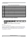
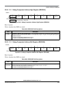
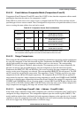
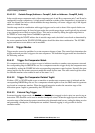
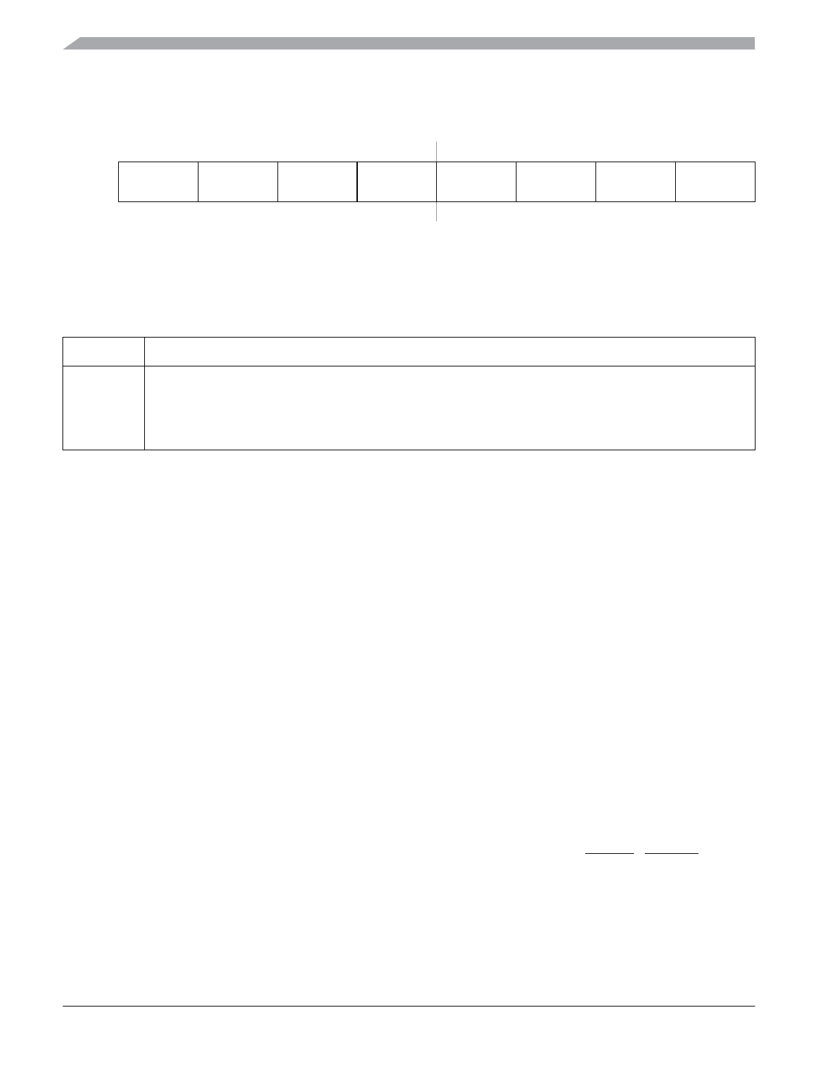
0x002F
76543210
R
Bit 7 6 5 4 3 2 1 Bit 0
W
Reset 00000000
Figure 20-21. Debug Comparator Data Low Mask Register (DBGXDLM)
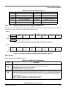
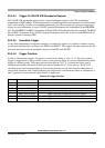
Table 20-35. DBGXDLM Field Descriptions
Field Description
7–0
Bits [7:0]
Comparator Data Low Mask Bits — The comparator data low mask bits control whether the selected
comparator compares the data bus bits [7:0] to the corresponding comparator data compare bits. This register
is available only for comparators A and C.
0 Do not compare corresponding data bit
1 Compare corresponding data bit