


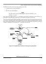

Chapter 15 Serial Communication Interface (S12MC9S12XDP512V5)
MC9S12XDP512 Data Sheet, Rev. 2.11
Freescale Semiconductor 675
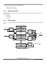
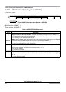
15.2 External Signal Description
The SCI module has a total of two external pins.
15.2.1 TXD — Transmit Pin
The TXD pin transmits SCI (standard or infrared) data. It will idle high in either mode and is high
impedance anytime the transmitter is disabled.
15.2.2 RXD — Receive Pin
The RXD pin receives SCI (standard or infrared) data. An idle line is detected as a line high. This input is
ignored when the receiver is disabled and should be terminated to a known voltage.
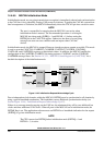
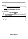
15.3 Memory Map and Register Definition
This section provides a detailed description of all the SCI registers.
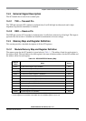
15.3.1 Module Memory Map and Register Definition
The memory map for the SCI module is given below in Table 1-1. The address listed for each register is
the address offset. The total address for each register is the sum of the base address for the SCI module and
the address offset for each register.
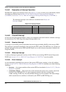
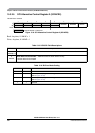
Table 15-1. MC9S12XDP512 Memory Map
Address
Offset
Name Access
0x0000
1
1
Those registers are accessible if the AMAP bit in the SCISR2 register is set to zero
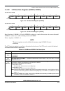
SCI Baud Rate Register High (SCIBDH) R/W
0x0001
1
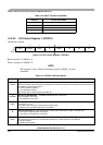
SCI Baud Rate Register Low (SCIBDL) R/W
0x0002
1
SCI Control Register1 (SCICR1) R/W
0x000a
2
2
Those registers are accessible if the AMAP bit in the SCISR2 register is set to one
SCI Alternative Status Register 1 (SCIASR1) R/W
0x001a
2
SCI Alternative Control Register 1 (SCIACR1) R/W
0x002a
2
SCI Alternative Control Register 2 (SCIACR2) R/W
0x0003 SCI Control Register 2 (SCICR2) R/W
0x0004 SCI Status Register 1 (SCISR1) R
0x0005 SCI Status Register 2(SCISR2) R/W
0x0006 SCI Data Register High (SCIDRH) R/W
0x0007 SCI Data Register Low (SCIDRL) R/W