


Chapter 4 Port Integration Module (S12XDP512PIMV2)
MC9S12XDP512 Data Sheet, Rev. 2.11
190 Freescale Semiconductor
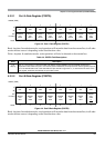
4.3.2 Register Descriptions
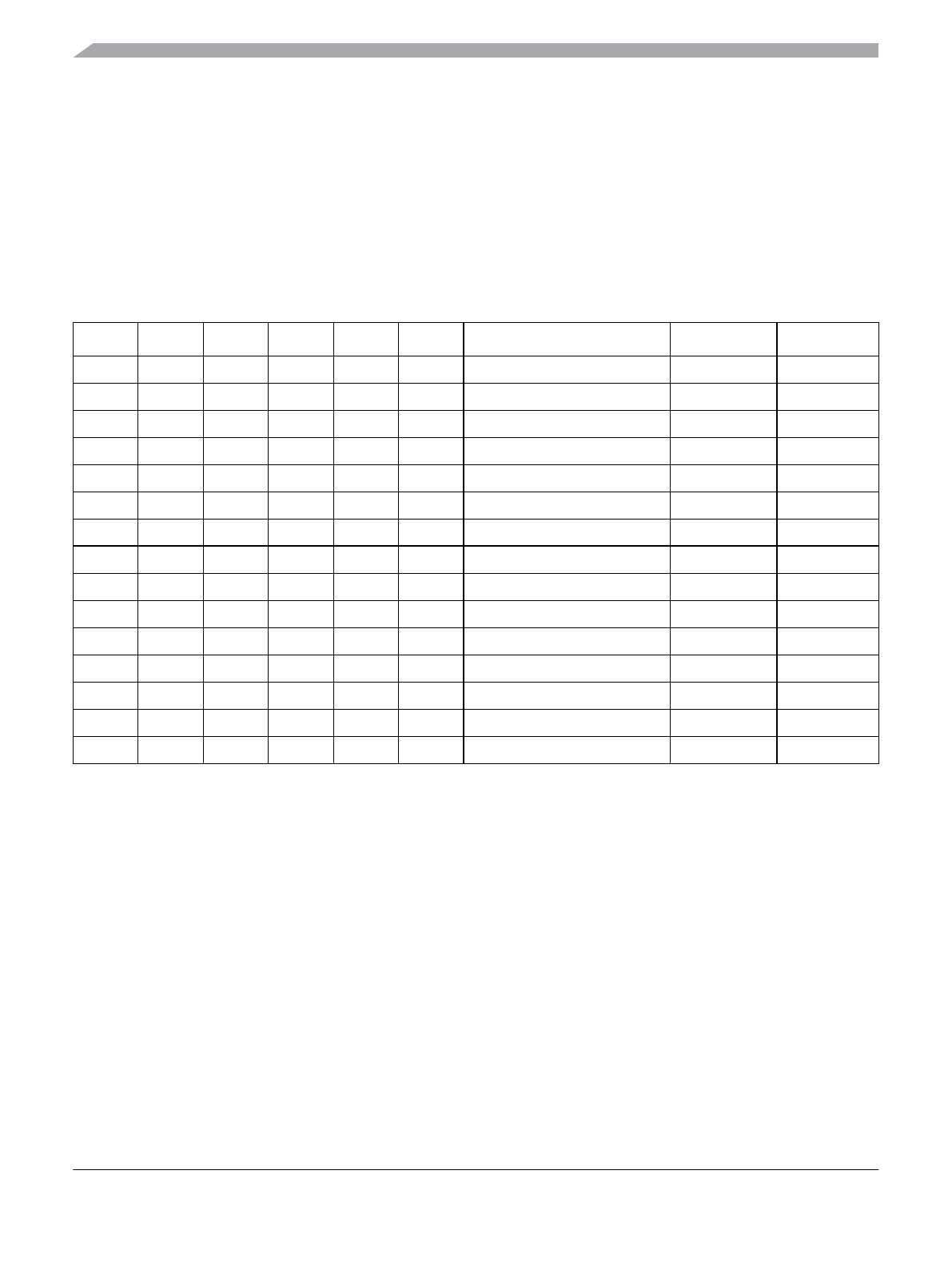
Table 4-3 summarizes the effect on the various configuration bits, data direction (DDR), output level (IO),
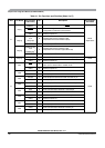
reduced drive (RDR), pull enable (PE), pull select (PS), and interrupt enable (IE) for the ports.
The configuration bit PS is used for two purposes:
1. Configure the sensitive interrupt edge (rising or falling), if interrupt is enabled.
2. Select either a pull-up or pull-down device if PE is active.
NOTE
All register bits in this module are completely synchronous to internal
clocks during a register read.
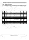
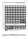
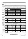
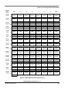
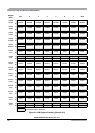
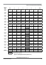
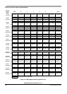
Table 4-3. Pin Configuration Summary
DDR IO RDR PE PS
1
1
Always “0” on Port A, B, C, D, E, K, AD0, and AD1.
IE
2
2
Applicable only on Port P, H, and J.
Function Pull Device Interrupt
0 x x 0 x 0 Input Disabled Disabled
0 x x 1 0 0 Input Pull Up Disabled
0 x x 1 1 0 Input Pull Down Disabled
0 x x 0 0 1 Input Disabled Falling edge
0 x x 0 1 1 Input Disabled Rising edge
0 x x 1 0 1 Input Pull Up Falling edge
0 x x 1 1 1 Input Pull Down Rising edge
1 0 0 x x 0 Output, full drive to 0 Disabled Disabled
1 1 0 x x 0 Output, full drive to 1 Disabled Disabled
1 0 1 x x 0 Output, reduced drive to 0 Disabled Disabled
1 1 1 x x 0 Output, reduced drive to 1 Disabled Disabled
1 0 0 x 0 1 Output, full drive to 0 Disabled Falling edge
1 1 0 x 1 1 Output, full drive to 1 Disabled Rising edge
1 0 1 x 0 1 Output, reduced drive to 0 Disabled Falling edge
1 1 1 x 1 1 Output, reduced drive to 1 Disabled Rising edge