


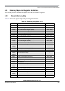
Chapter 4 Port Integration Module (S12XDP512PIMV2)
MC9S12XDP512 Data Sheet, Rev. 2.11
Freescale Semiconductor 181
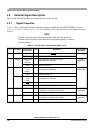
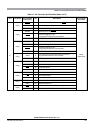
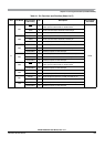
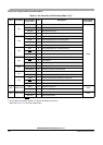
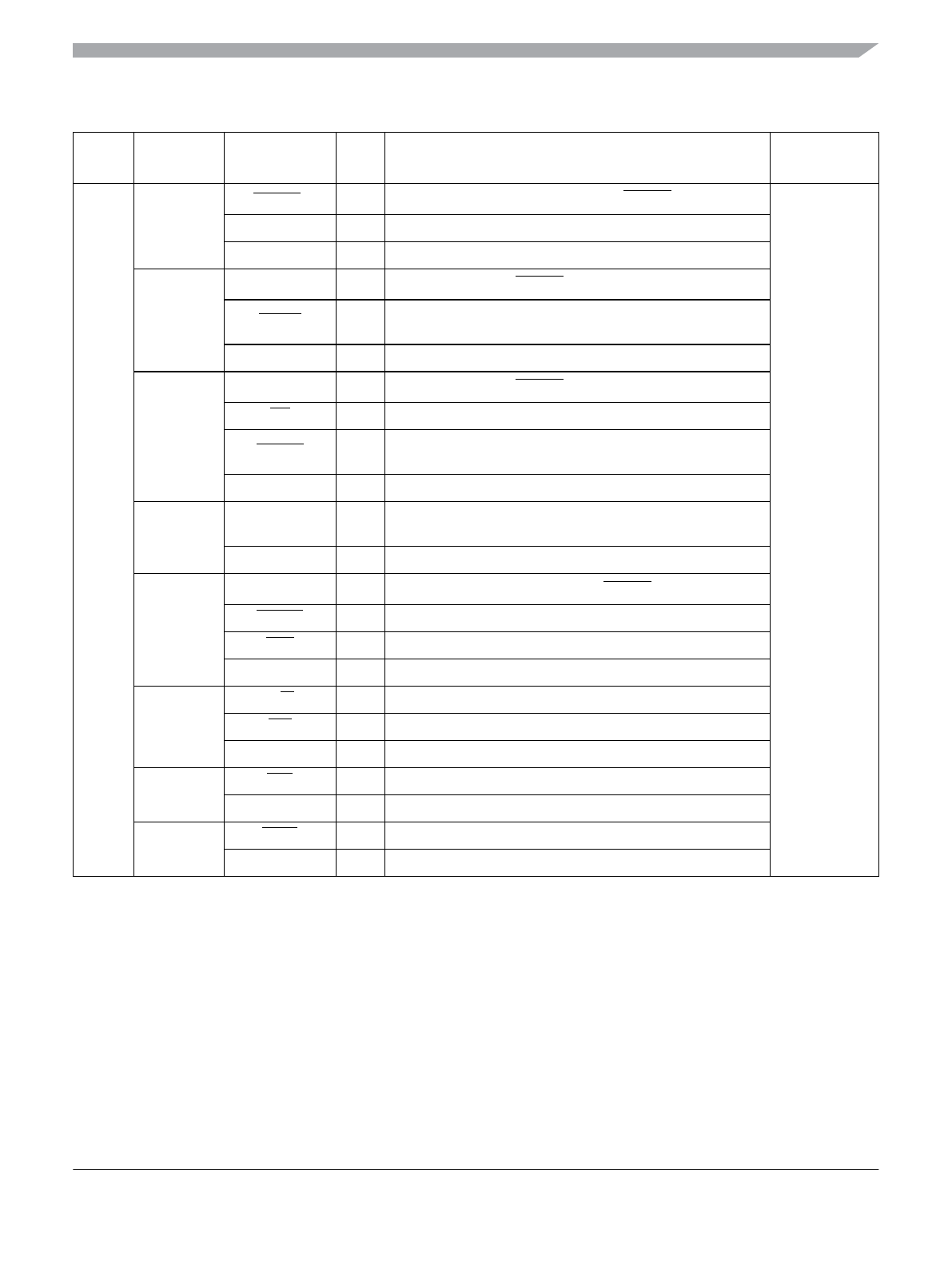
E
PE[7]
XCLKS
1
I External clock selection input during RESET
Mode
dependent
3
ECLKX2 I Free-running clock output at Core Clock rate (ECLK x 2)
GPIO I/O General-purpose I/O
PE[6]
MODB
1
I MODB input during RESET
TAGHI I
Instruction tagging low pin
Configurable for reduced input threshold
GPIO I/O General-purpose I/O
PE[5]
MODA
1
I MODA input during RESET
RE O Read enable signal
TAGLO I
Instruction tagging low pin
Configurable for reduced input threshold
GPIO I/O General-purpose I/O
PE[4]
ECLK O
Free-running clock output at the Bus Clock rate or
programmable divided in normal modes
GPIO I/O General-purpose I/O
PE[3]
EROMCTL
1
I EROMON bit control input during RESET
LSTRB O Low strobe bar output
LDS O Lower data strobe
GPIO I/O General-purpose I/O
PE[2]
R/
W O Read/write output for external bus
WE O Write enable signal
GPIO I/O General-purpose I/O
PE[1]
IRQ I Maskable level- or falling edge-sensitive interrupt input
GPIO I/O General-purpose I/O
PE[0]
XIRQ I Non-maskable level-sensitive interrupt input
GPIO I/O General-purpose I/O
Table 4-1. Pin Functions and Priorities (Sheet 2 of 7)
Port Pin Name
Pin Function
and Priority
I/O Description
Pin Function
after Reset