


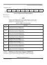
Chapter 12 Pulse-Width Modulator (S12PWM8B8CV1)
MC9S12XDP512 Data Sheet, Rev. 2.11
Freescale Semiconductor 569
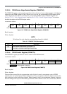
Read: Anytime
Write: Anytime
NOTE
Register bits PCLK0 to PCLK7 can be written anytime. If a clock select is
changed while a PWM signal is being generated, a truncated or stretched
pulse can occur during the transition.
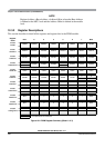
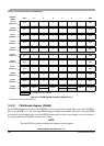
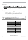
12.3.2.4 PWM Prescale Clock Select Register (PWMPRCLK)
This register selects the prescale clock source for clocks A and B independently.
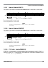
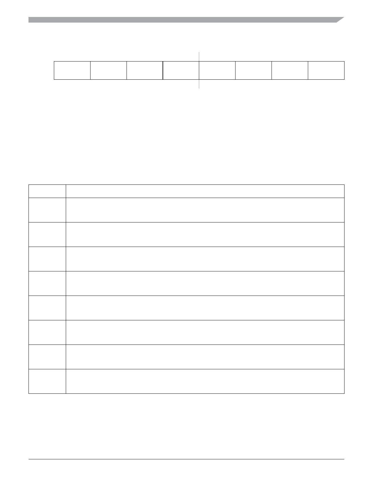
Module Base + 0x0002
76543210
R
PCLK7 PCLKL6 PCLK5 PCLK4 PCLK3 PCLK2 PCLK1 PCLK0
W
Reset 00000000
Figure 12-5. PWM Clock Select Register (PWMCLK)
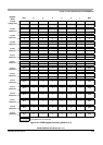
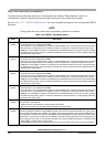
Table 12-3. PWMCLK Field Descriptions
Field Description
7
PCLK7
Pulse Width Channel 7 Clock Select
0 Clock B is the clock source for PWM channel 7.
1 Clock SB is the clock source for PWM channel 7.
6
PCLK6
Pulse Width Channel 6 Clock Select
0 Clock B is the clock source for PWM channel 6.
1 Clock SB is the clock source for PWM channel 6.
5
PCLK5
Pulse Width Channel 5 Clock Select
0 Clock A is the clock source for PWM channel 5.
1 Clock SA is the clock source for PWM channel 5.
4
PCLK4
Pulse Width Channel 4 Clock Select
0 Clock A is the clock source for PWM channel 4.
1 Clock SA is the clock source for PWM channel 4.
3
PCLK3
Pulse Width Channel 3 Clock Select
0 Clock B is the clock source for PWM channel 3.
1 Clock SB is the clock source for PWM channel 3.
2
PCLK2
Pulse Width Channel 2 Clock Select
0 Clock B is the clock source for PWM channel 2.
1 Clock SB is the clock source for PWM channel 2.
1
PCLK1
Pulse Width Channel 1 Clock Select
0 Clock A is the clock source for PWM channel 1.
1 Clock SA is the clock source for PWM channel 1.
0
PCLK0
Pulse Width Channel 0 Clock Select
0 Clock A is the clock source for PWM channel 0.
1 Clock SA is the clock source for PWM channel 0.