


Chapter 14 Freescale’s Scalable Controller Area Network (S12MSCANV3)
MC9S12XDP512 Data Sheet, Rev. 2.11
Freescale Semiconductor 627
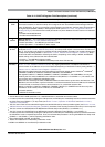
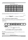
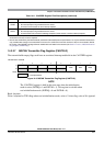
14.3.2.4 MSCAN Bus Timing Register 1 (CANBTR1)
The CANBTR1 register configures various CAN bus timing parameters of the MSCAN module.
Read: Anytime
Write: Anytime in initialization mode (INITRQ = 1 and INITAK = 1)
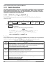
Module Base + 0x0003
76543210
R
SAMP TSEG22 TSEG21 TSEG20 TSEG13 TSEG12 TSEG11 TSEG10
W
Reset: 00000000
Figure 14-6. MSCAN Bus Timing Register 1 (CANBTR1)
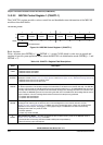
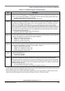
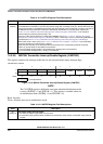
Table 14-7. CANBTR1 Register Field Descriptions
Field Description
7
SAMP
Sampling — This bit determines the number of CAN bus samples taken per bit time.
0 One sample per bit.
1 Three samples per bit
1
.
If SAMP = 0, the resulting bit value is equal to the value of the single bit positioned at the sample point. If
SAMP = 1, the resulting bit value is determined by using majority rule on the three total samples. For higher bit
rates, it is recommended that only one sample is taken per bit time (SAMP = 0).
1
In this case, PHASE_SEG1 must be at least 2 time quanta (Tq).
6:4
TSEG2[2:0]
Time Segment 2 — Time segments within the bit time fix the number of clock cycles per bit time and the location
of the sample point (see Figure 14-43). Time segment 2 (TSEG2) values are programmable as shown in
Table 14-8.
3:0
TSEG1[3:0]
Time Segment 1 — Time segments within the bit time fix the number of clock cycles per bit time and the location
of the sample point (see Figure 14-43). Time segment 1 (TSEG1) values are programmable as shown in
Table 14-9.
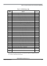
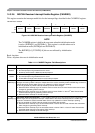
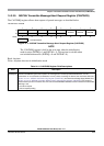
Table 14-8. Time Segment 2 Values
TSEG22 TSEG21 TSEG20 Time Segment 2
0 0 0 1 Tq clock cycle
1
1
This setting is not valid. Please refer to Table 14-36 for valid settings.
0 0 1 2 Tq clock cycles
::: :
1 1 0 7 Tq clock cycles
1 1 1 8 Tq clock cycles