


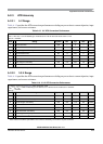
Appendix A Electrical Characteristics
MC9S12XDP512 Data Sheet, Rev. 2.11
Freescale Semiconductor 943
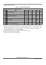
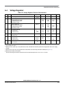
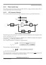
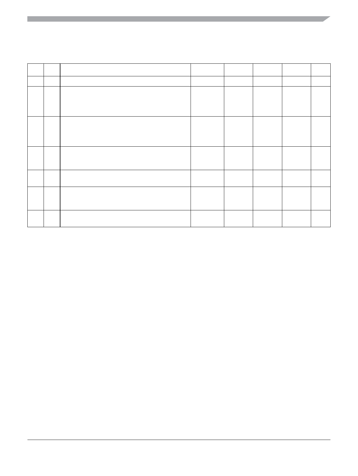
A.4 Voltage Regulator
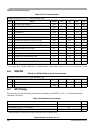
Table A-19. Voltage Regulator Electrical Characteristics
Num C Characteristic Symbol Min Typ Max Unit
1 P Input voltages V
VDDR,A
3.15 — 5.5 V
3 P Output voltage core
Full performance mode
Reduced power mode
Shutdown mode
V
DD
2.35
1.4
—
2.54
2.25
—
1
1
High impedance output
2.75
2.75
—
V
V
V
4 P Output Voltage PLL
Full Performance Mode
Reduced power mode
Shutdown mode
V
DDPLL
2.35
1.25
—
2.54
2.25
—
2
2
High impedance output
2.75
2.75
—
V
V
V
7 P Low-voltage interrupt
3
Assert level
Deassert level
3
Monitors V
DDA
, active only in full performance mode. Indicates I/O and ADC performance degradation due to low supply
voltage.
V
LVIA
V
LVID
4.0
4.15
4.37
4.52
4.66
4.77
V
V
8 P Low-voltage reset
4
Assert level
4
Monitors V
DD
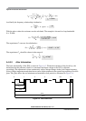
, active only in full performance mode. MCU is monitored by the POR in RPM (see Figure A-1)
V
LVRA
2.25 — — V
9 C Power-on reset
5
Assert level
Deassert level
5
Monitors V
DD
. Active in all modes.
V
PORA
V
PORD
0.97
—
—
—
—
2.05
V
V
12 C Trimmed API internal clock
6
∆f / f
nominal
6
The API Trimming bits must be set that the minimum periode equals to 0.2 ms. f
nominal
= 1/0.2ms
df
API
– 10% — + 10% —