


Chapter 4 Port Integration Module (S12XDP512PIMV2)
MC9S12XDP512 Data Sheet, Rev. 2.11
262 Freescale Semiconductor
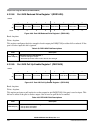
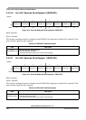
4.4.1.8 Interrupt Enable Register
If the pin is used as an interrupt input this register serves as a mask to the interrupt flag to enable/disable
the interrupt.
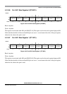
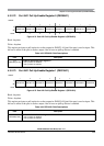
4.4.1.9 Interrupt Flag Register
If the pin is used as an interrupt input this register holds the interrupt flag after a valid pin event.
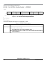
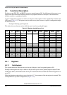
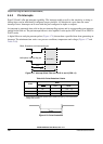
4.4.1.10 Module Routing Register
This register supports the re-routing of the CAN0, CAN4, SPI0, SPI1, and SPI2 pins to alternative ports.
This allows a software re-configuration of the pinouts of the different package options with respect to
above peripherals.
NOTE
The purpose of the module routing register is to provide maximum
flexibility for derivatives with a lower number of MSCAN and SPI modules.
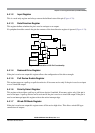
4.4.2 Ports
4.4.2.1 BKGD Pin
The BKGD pin is associated with the S12X_BDM and S12X_EBI modules. During reset, the BKGD pin
is used as MODC input.
4.4.2.2 Port A and B
Port A pins PA[7:0] and Port B pins PB[7:0] can be used for either general-purpose I/O, or, in 144-pin
packages, also with the external bus interface. In this case port A and port B are associated with the
external address bus outputs ADDR15–ADDR8 and ADDR7–ADDR0, respectively. PB0 is the ADDR0
or
UDS output.
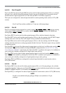
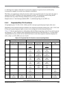
Table 4-68. Module Implementations on Derivatives
Number
of Modules
MSCAN Modules SPI Modules
CAN0 CAN1 CAN2 CAN3 CAN4 SPI0 SPI1 SPI2
5 yes yes yes yes yes — — —
4 yes yes yes — yes — — —
3 yes yes — — yes yes yes yes
2 yes — — — yes yes yes —
1 yes————yes——