


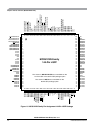
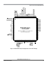
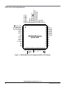

Chapter 1 Device Overview (MC9S12XDP512V2)
MC9S12XDP512 Data Sheet, Rev. 2.11
80 Freescale Semiconductor
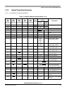
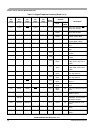
1.2.3.11 PB0 / ADDR0 / UDS / IVD[0] — Port B I/O Pin 0
PB0 is a general-purpose input or output pin. In MCU expanded modes of operation, this pin is used for
the external address bus ADDR0 or as upper data strobe signal. In MCU emulation modes of operation,
this pin is used for external address bus ADDR0 and internal visibility read data IVD0.
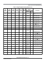
1.2.3.12 PC[7:0] / DATA [15:8] — Port C I/O Pins
PC[7:0] are general-purpose input or output pins. In MCU expanded modes of operation, these pins are
used for the external data bus.
The input voltage thresholds for PC[7:0] can be configured toreduced levels, to allow data from an external
3.3-V peripheral to be read by the MCU operating at 5.0 V. The input voltage thresholds for PC[7:0] are
configured to reduced levels out of reset in expanded and emulation modes. The input voltage thresholds
for PC[7:0] are configured to 5-V levels out of reset in normal modes.
1.2.3.13 PD[7:0] / DATA [7:0] — Port D I/O Pins
PD[7:0] are general-purpose input or output pins. In MCU expanded modes of operation, these pins are
used for the external data bus.
The input voltage thresholds for PD[7:0] can be configured to reduced levels, to allow data from an
external 3.3-V peripheral to be read by the MCU operating at 5.0 V. The input voltage thresholds for
PD[7:0] are configured to reduced levels out of reset in expanded and emulation modes. The input voltage
thresholds for PC[7:0] are configured to 5-V levels out of reset in normal modes.
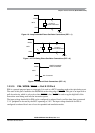
1.2.3.14 PE7 / ECLKX2 / XCLKS — Port E I/O Pin 7
PE7 is a general-purpose input or output pin. The XCLKS is an input signal which controls whether a
crystal in combination with the internal loop controlled (low power) Pierce oscillator is used or whether
full swing Pierce oscillator/external clock circuitry is used.
The
XCLKS signal selects the oscillator configuration during reset low phase while a clock quality check
is ongoing. This is the case for:
• Power on reset or low-voltage reset
• Clock monitor reset
• Any reset while in self-clock mode or full stop mode
The selected oscillator configuration is frozen with the rising edge of reset.
The pin can be configured to drive the internal system clock ECLKX2.