


Appendix A Electrical Characteristics
MC9S12XDP512 Data Sheet, Rev. 2.11
950 Freescale Semiconductor
A.6 MSCAN
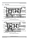
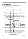
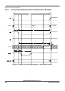
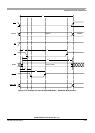
A.7 SPI Timing
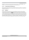
This section provides electrical parametrics and ratings for the SPI. In Table A-24 the measurement
conditions are listed.
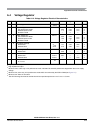
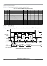
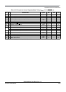
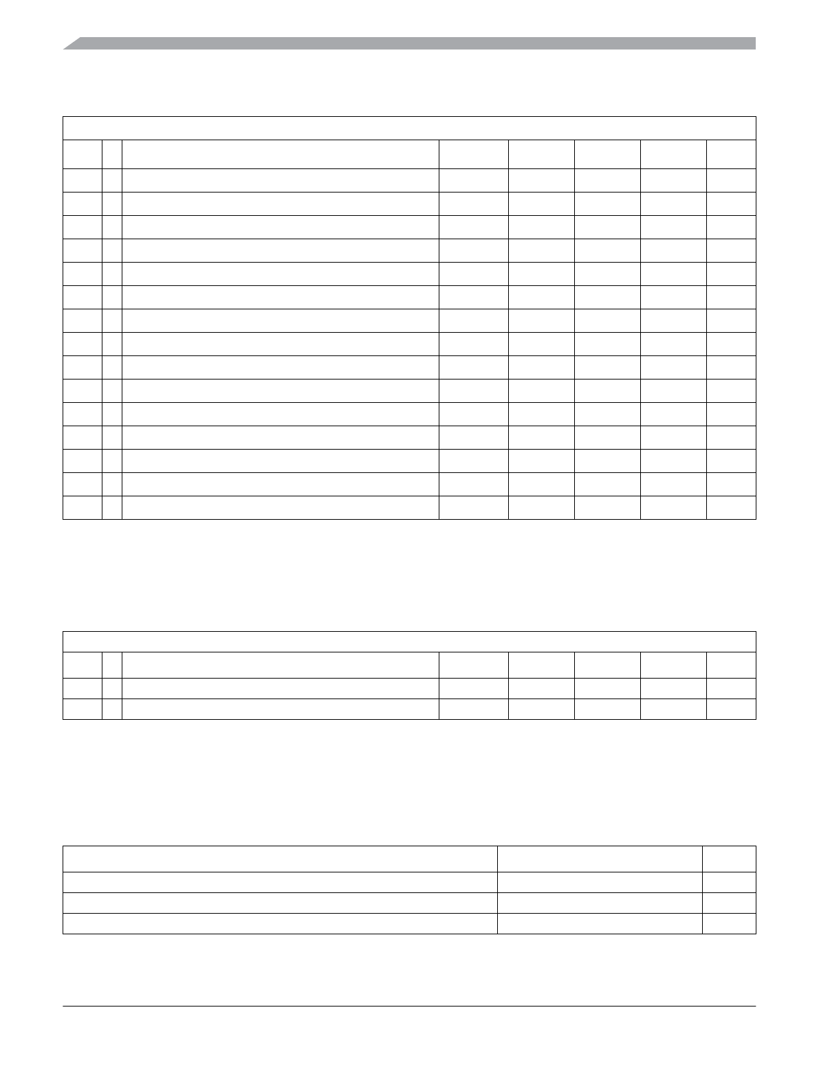
Table A-22. PLL Characteristics
Conditions are shown in Table A-4 unless otherwise noted
Num C Rating Symbol Min Typ Max Unit
1 P Self clock mode frequency f
SCM
1 — 5.5 MHz
2 D VCO locking range f
VCO
8 — 80 MHz
3 D Lock detector transition from acquisition to tracking mode |∆
trk
|3 — 4%
1
1
% deviation from target frequency
4 D Lock detection |∆
Lock
| 0 — 1.5 %
1
5 D Unlock detection |∆
unl
| 0.5 — 2.5 %
1
6 D Lock detector transition from tracking to acquisition mode |∆
unt
|6 — 8%
1
7 C PLLON total stabilization delay (auto mode)
2
2
f
osc
= 4 MHz, f
BUS
= 40 MHz equivalent f
VCO
= 80 MHz: REFDV = #$00, SYNR = #$09, C
S
= 4.7 nF, C
P
= 470 pF, R
S
= 4.7 kΩ
t
stab
— 0.24 — ms
8 D PLLON acquisition mode stabilization delay
2
t
acq
— 0.09 — ms
9 D PLLON tracking mode stabilization delay
2
t
al
— 0.16 — ms
10 D Fitting parameter VCO loop gain K
1
— –195 — MHz/V
11 D Fitting parameter VCO loop frequency f
1
— 126 — MHz
12 D Charge pump current acquisition mode | i
ch
| — 38.5 — µA
13 D Charge pump current tracking mode | i
ch
| — 3.5 — µA
14 C Jitter fit parameter 1
2
j
1
— 0.9 1.3 %
15 C Jitter fit parameter 2
2
j
2
— 0.02 0.12 %
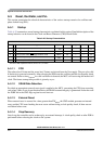
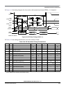
Table A-23. MSCAN Wake-up Pulse Characteristics
Conditions are shown in Table A-4 unless otherwise noted
Num C Rating Symbol Min Typ Max Unit
1 P MSCAN wakeup dominant pulse filtered t
WUP
—— 2µs
2 P MSCAN wakeup dominant pulse pass t
WUP
5——µs
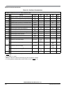
Table A-24. Measurement Conditions
Description Value Unit
Drive mode Full drive mode —
Load capacitance C
LOAD
1
,
on all outputs
1
Timing specified for equal load on all SPI output pins. Avoid asymmetric load.
50 pF
Thresholds for delay measurement points (20% / 80%) V
DDX
V