


Chapter 9 XGATE (S12XGATEV2)
MC9S12XDP512 Data Sheet, Rev. 2.11
Freescale Semiconductor 379
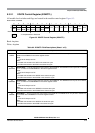
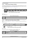
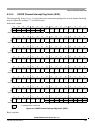
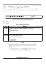
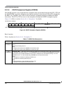
9.3.2.1 XGATE Control Register (XGMCTL)
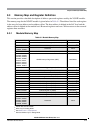
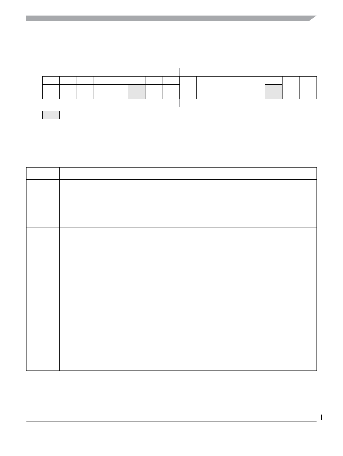
All module level switches and flags are located in the module control register Figure 9-3.
Read: Anytime
Write: Anytime
Module Base +0x00000
15 14 13 12 11 10 9 8 7 6 5 4 3 2 1 0
R00000000
XGE XGFRZ XGDBG XGSS XGFACT
0
XG
SWEIF
XGIE
W
XGEM
XG
FRZM
XG
DBGM
XG
SSM
XG
FACTM
XG
SWEIFM
XGIEM
Reset 0 0 0 0000000000000
= Unimplemented or Reserved
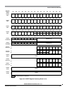
Figure 9-3. XGATE Control Register (XGMCTL)
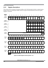
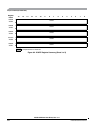
Table 9-2. XGMCTL Field Descriptions (Sheet 1 of 3)
Field Description
15
XGEM
XGE Mask — This bit controls the write access to the XGE bit. The XGE bit can only be set or cleared if a "1" is
written to the XGEM bit in the same register access.
Read:
This bit will always read "0".
Write:
0 Disable write access to the XGE in the same bus cycle
1 Enable write access to the XGE in the same bus cycle
14
XGFRZM
XGFRZ Mask — This bit controls the write access to the XGFRZ bit. The XGFRZ bit can only be set or cleared
if a "1" is written to the XGFRZM bit in the same register access.
Read:
This bit will always read "0".
Write:
0 Disable write access to the XGFRZ in the same bus cycle
1 Enable write access to the XGFRZ in the same bus cycle
13
XGDBGM
XGDBG Mask — This bit controls the write access to the XGDBG bit. The XGDBG bit can only be set or cleared
if a "1" is written to the XGDBGM bit in the same register access.
Read:
This bit will always read "0".
Write:
0 Disable write access to the XGDBG in the same bus cycle
1 Enable write access to the XGDBG in the same bus cycle
12
XGSSM
XGSS Mask — This bit controls the write access to the XGSS bit. The XGSS bit can only be set or cleared if a
"1" is written to the XGSSM bit in the same register access.
Read:
This bit will always read "0".
Write:
0 Disable write access to the XGSS in the same bus cycle
1 Enable write access to the XGSS in the same bus cycle