


Chapter 7 Analog-to-Digital Converter (ATD10B16CV4)
MC9S12XDP512 Data Sheet, Rev. 2.11
342 Freescale Semiconductor
7.3.2.16.2 Right Justified Result Data
7.4 Functional Description
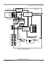
The ATD10B16C is structured in an analog and a digital sub-block.
7.4.1 Analog Sub-block
The analog sub-block contains all analog electronics required to perform a single conversion. Separate
power supplies V
DDA
and V
SSA
allow to isolate noise of other MCU circuitry from the analog sub-block.
7.4.1.1 Sample and Hold Machine
The sample and hold (S/H) machine accepts analog signals from the external world and stores them as
capacitor charge on a storage node.
The sample process uses a two stage approach. During the first stage, the sample amplifier is used to
quickly charge the storage node.The second stage connects the input directly to the storage node to
complete the sample for high accuracy.
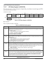
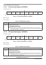
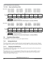
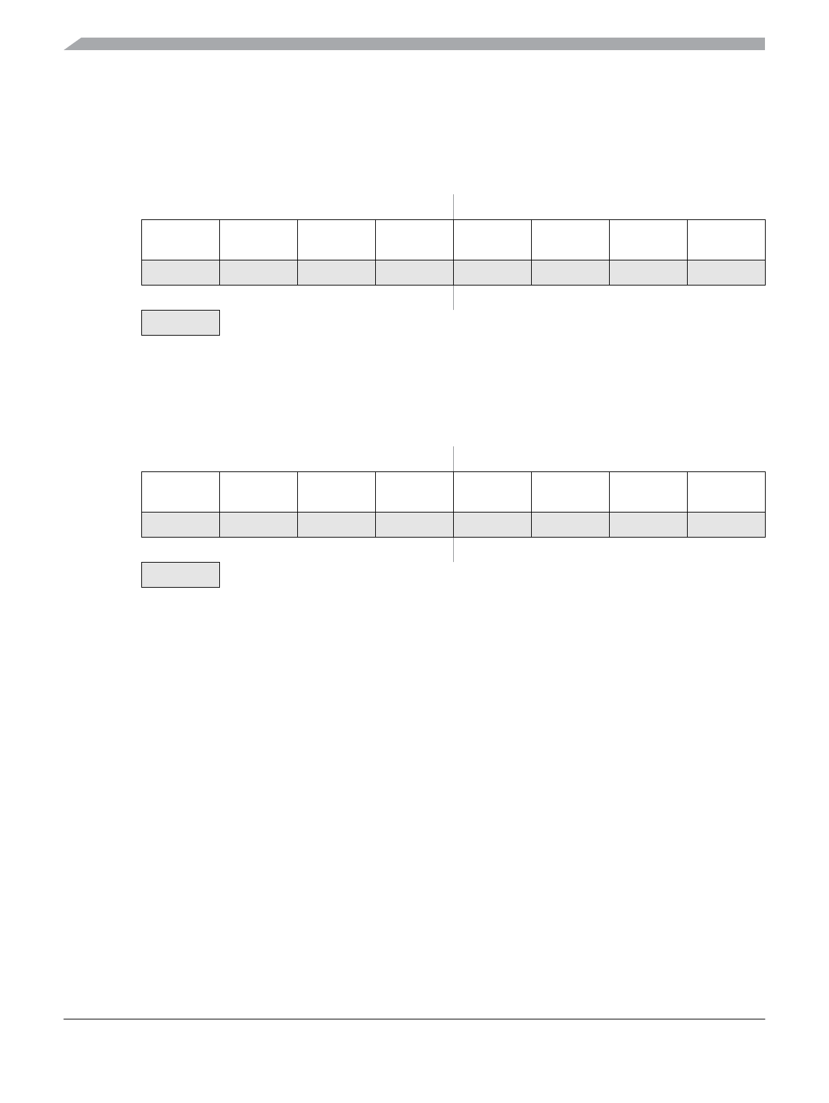
Module Base + 0x0010 = ATDDR0H,
0x0012 = ATDDR1H,
0x0014 = ATDDR2H,
0x0016 = ATDDR3H
0x0018 = ATDDR4H,
0x001A = ATDDR5H,
0x001C = ATDDR6H,
0x001E = ATDDR7H
0x0020 = ATDDR8H,
0x0022 = ATDDR9H,
0x0024 = ATDDR10H,
0x0026 = ATDDR11H
0x0028 = ATDDR12H,
0x002A = ATDDR13H,
0x002C = ATDDR14H,
0x002E = ATDDR15H
76543210
R (10-BIT)
R (8-BIT)
0
0
0
0
0
0
0
0
0
0
0
0
BIT 9 MSB
0
BIT 8
0
W
Reset 00000000
= Unimplemented or Reserved
Figure 7-20. Right Justified, ATD Conversion Result Register x, High Byte (ATDDRxH)
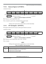
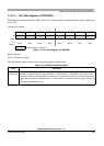
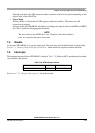
Module Base + 0x0011 = ATDDR0L,
0x0013 = ATDDR1L,
0x0015 = ATDDR2L,
0x0017 = ATDDR3L
0x0019 = ATDDR4L,
0x001B = ATDDR5L,
0x001D = ATDDR6L,
0x001F = ATDDR7L
0x0021 = ATDDR8L,
0x0023 = ATDDR9L,
0x0025 = ATDDR10L,
0x0027 = ATDDR11L
0x0029 = ATDDR12L,
0x002B = ATDDR13L,
0x002D = ATDDR14L,
0x002F = ATDDR15L
76543210
R (10-BIT)
R (8-BIT)
BIT 7
BIT 7 MSB
BIT 6
BIT 6
BIT 5
BIT 5
BIT 4
BIT 4
BIT 3
BIT 3
BIT 2
BIT 2
BIT 1
BIT 1
BIT 0
BIT 0
W
Reset 00000000
= Unimplemented or Reserved
Figure 7-21. Right Justified, ATD Conversion Result Register x, Low Byte (ATDDRxL)