


Chapter 20 Debug (S12XDBGV2)
MC9S12XDP512 Data Sheet, Rev. 2.11
Freescale Semiconductor 807
20.3.1.11.1 Debug Comparator Control Register (DBGXCTL)
The contents of this register bits 7 and 6 differ depending upon which comparator registers are visible in
the 8-byte window of the DBG module register address map
Read: Anytime
Write: Anytime when DBG not armed.
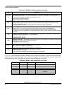
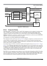
0x0029 ADDRESS HIGH Read/Write
0x002A ADDRESS MEDIUM Read/Write
0x002B ADDRESS LOW Read/Write
0x002C DATA HIGH COMPARATOR Read/Write Comparator A and C only
0x002D DATA LOW COMPARATOR Read/Write Comparator A and C only
0x002E DATA HIGH MASK Read/Write Comparator A and C only
0x002F DATA LOW MASK Read/Write Comparator A and C only
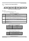
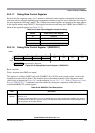
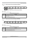
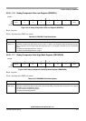
0x0028
76543210
R0
NDB TAG BRK RW RWE SRC COMPE
W
Reset 00000000
Unimplemented or Reserved
Figure 20-13. Debug Comparator Control Register (Comparators A and C)
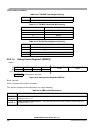
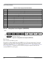
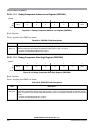
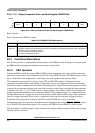
0x0028
76543210
R
SZE SZ TAG BRK RW RWE SRC COMPE
W
Reset 00000000
Figure 20-14. Debug Comparator Control Register (Comparators B and D)
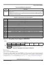
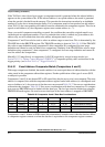
Table 20-27. DBGXCTL Field Descriptions
Field Description
7
(COMPB/D)
SZE
Size Comparator Enable Bit — The SZE bit controls whether access size comparison is enabled for the
associated comparator. This bit is ignored if the TAG bit in the same register is set.
0 Word/Byte access size is not used in comparison
1 Word/Byte access size is used in comparison
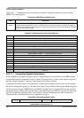
6
(COMPA/C)
NDB
Not Data Bus Compare — The NDB bit controls whether the match occurs when the data bus matches the
comparator register value or when the data bus differs from the register value. Furthermore database bits can
be individually masked using the comparator data mask registers. This bit is only available for comparators A
and C. This bit is ignored if the TAG bit in the same register is set. This bit position has an SZ functionality for
comparators B and D.
0 Match on data bus equivalence to comparator register contents
1 Match on data bus difference to comparator register contents
Table 20-26. Comparator Register Layout