


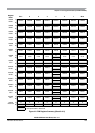
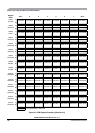
Chapter 4 Port Integration Module (S12XDP512PIMV2)
MC9S12XDP512 Data Sheet, Rev. 2.11
Freescale Semiconductor 199
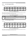
4.3.2.3 Port A Data Direction Register (DDRA)
Read: Anytime. In emulation modes, read operations will return the data from the external bus, in all other
modes the data are read from this register.
Write: Anytime. In emulation modes, write operations will also be directed to the external bus.
4.3.2.4 Port B Data Direction Register (DDRB)
Read: Anytime. In emulation modes, read operations will return the data from the external bus, in all other
modes the data are read from this register.
Write: Anytime. In emulation modes, write operations will also be directed to the external bus.
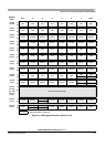
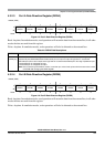
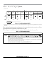
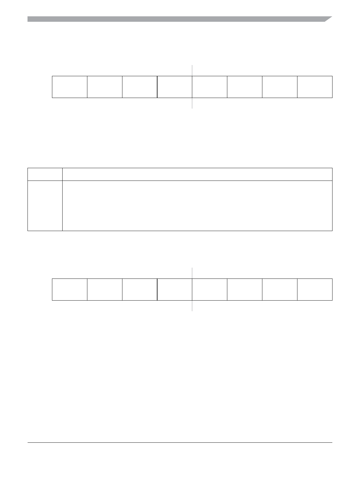
0x0002 (PRR)
76543210
R
DDRA7 DDRA6 DDRA5 DDRA4 DDRA3 DDRA2 DDRA1 DDRA0
W
Reset 00000000
Figure 4-5. Port A Data Direction Register (DDRA)
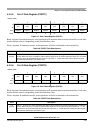
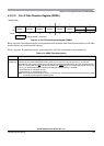
Table 4-6. DDRA Field Descriptions
Field Description
7–0
DDRA[7:0]
Data Direction Port A — This register controls the data direction for portA. When Port A is operating as a general
purpose I/O port, DDRA determines whether each pin is an input or output. A logic level “1” causes the
associated port pin to be an output and a logic level “0” causes the associated pin to be a high-impedance input.
0 Associated pin is configured as input.
1 Associated pin is configured as output.
Note: Due to internal synchronization circuits, it can take up to 2 bus clock cycles until the correct value is read
on PORTA after changing the DDRA register.
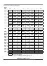
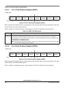
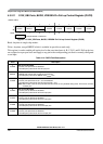
0x0003 (PRR)
76543210
R
DDRB7 DDRB6 DDRB5 DDRB4 DDRB3 DDRB2 DDRB1 DDRB0
W
Reset 00000000
Figure 4-6. Port B Data Direction Register (DDRB)