


Chapter 20 Debug (S12XDBGV2)
MC9S12XDP512 Data Sheet, Rev. 2.11
800 Freescale Semiconductor
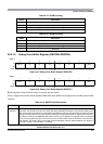
20.3.1.4 Debug Control Register2 (DBGC2)
Read: Anytime
Write: Anytime the module is disarmed.
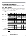
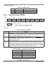
This register configures the comparators for range matching.
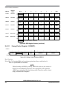
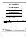
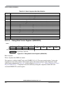
11 Trace only in range from comparator C to comparator D
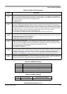
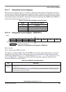
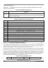
Table 20-11. TRCMOD Trace Mode Bit Encoding
TRCMOD Description
00 NORMAL
01 LOOP1
10 DETAIL
11 Reserved
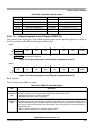
Table 20-12. TALIGN Trace Alignment Encoding
TALIGN Description
00 Trigger at end of stored data
01 Trigger before storing data
10 Trace buffer entries before and after trigger
11 Reserved
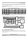
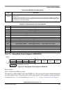
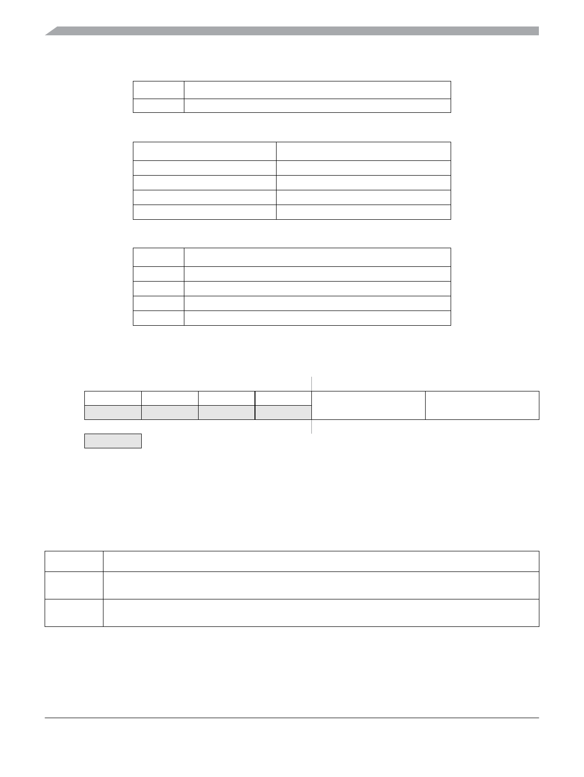
0x0023
76543210
R0000
CDCM ABCM
W
Reset 00000000
Unimplemented or Reserved
Figure 20-6. Debug Control Register2 (DBGC2)
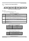
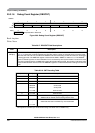
Table 20-13. DBGC2 Field Descriptions
Field Description
3–2
CDCM[3:2]
C and D Comparator Match Control — These bits determine the C and D comparator match mapping as
described in Table 20-14.
1–0
ABCM[1:0]
A and B Comparator Match Control — These bits determine the A and B comparator match mapping as
described in Table 20-15.
Table 20-10. TRANGE Trace Range Encoding
TRANGE Tracing Source