


512 Kbyte Flash Module (S12XFTX512K4V2)
BookTitle, Rev. 2.4
104 Freescale Semiconductor
2.3 Memory Map and Register Definition
This section describes the memory map and registers for the Flash module.
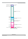
2.3.1 Module Memory Map
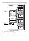
The Flash memory map is shown in Figure 2-2. The HCS12X architecture places the Flash memory
addresses between global addresses 0x78_0000 and 0x7F_FFFF. The FPROT register, described in
Section 2.3.2.5, “Flash Protection Register (FPROT)”, can be set to protect regions in the Flash memory
from accidental program or erase. Three separate memory regions, one growing upward from global
address 0x7F_8000 in the Flash memory (called the lower region), one growing downward from global
address 0x7F_FFFF in the Flash memory (called the higher region), and the remaining addresses in the
Flash memory, can be activated for protection. The Flash memory addresses covered by these protectable
regions are shown in the Flash memory map. The higher address region is mainly targeted to hold the boot
loader code since it covers the vector space. The lower address region can be used for EEPROM emulation
in an MCU without an EEPROM module since it can be left unprotected while the remaining addresses
are protected from program or erase. Default protection settings as well as security information that allows
the MCU to restrict access to the Flash module are stored in the Flash configuration field as described in
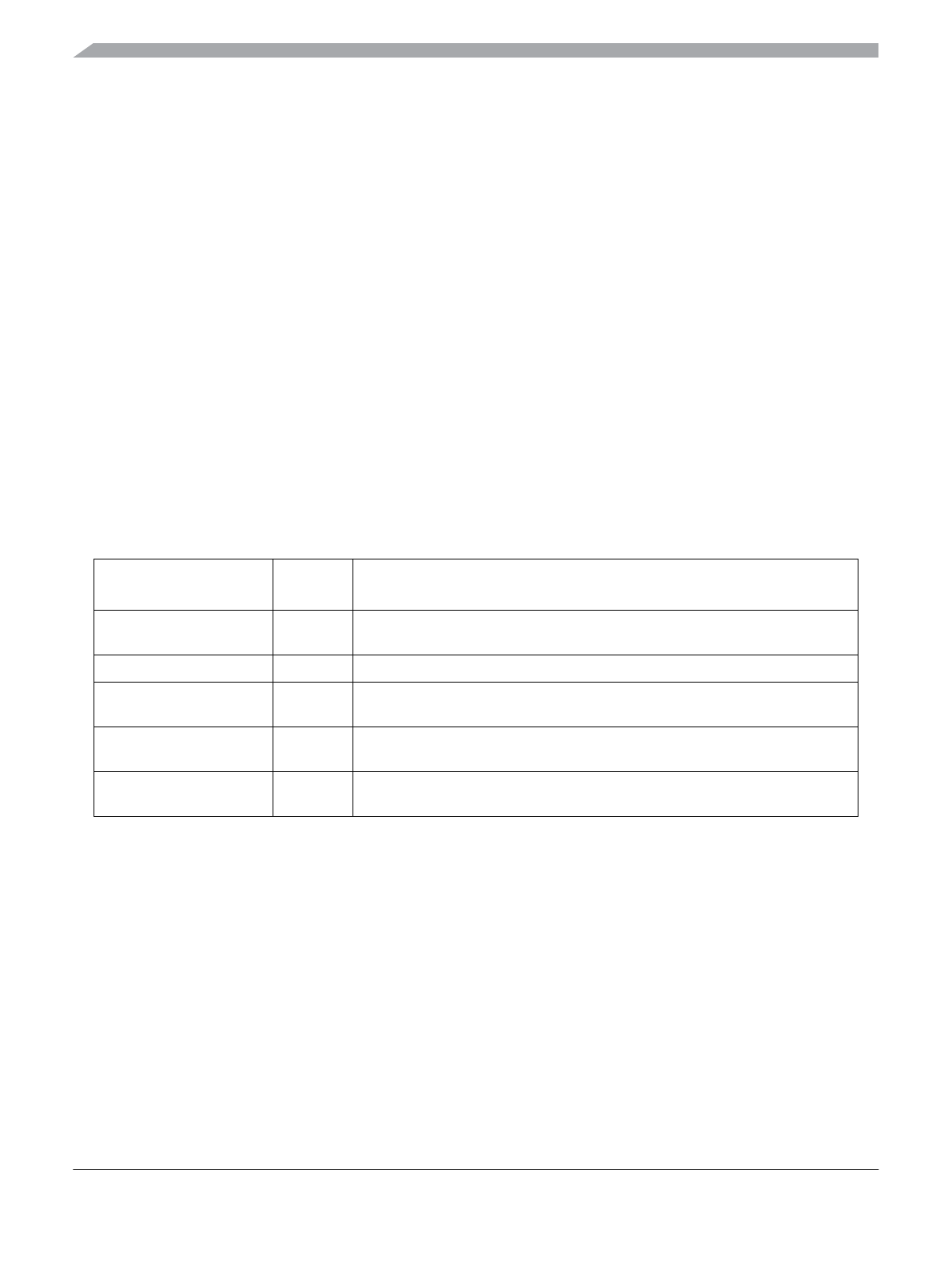
Table 2-1.
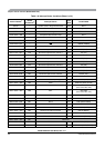
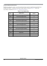
Table 2-1. Flash Configuration Field
Global Address
Size
(Bytes)
Description
0x7F_FF00 – 0x7F_FF07 8 Backdoor Comparison Key
Refer to Section 2.6.1, “Unsecuring the MCU using Backdoor Key Access”
0x7F_FF08 – 0x7F_FF0C 5 Reserved
0x7F_FF0D 1 Flash Protection byte
Refer to Section 2.3.2.5, “Flash Protection Register (FPROT)”
0x7F_FF0E 1 Flash Nonvolatile byte
Refer to Section 2.3.2.8, “Flash Control Register (FCTL)”
0x7F_FF0F 1 Flash Security byte
Refer to Section 2.3.2.2, “Flash Security Register (FSEC)”