


Chapter 15 Serial Communication Interface (S12MC9S12XDP512V5)
MC9S12XDP512 Data Sheet, Rev. 2.11
678 Freescale Semiconductor
15.3.2.2 SCI Control Register 1 (SCICR1)
Read: Anytime, if AMAP = 0.
Write: Anytime, if AMAP = 0.
NOTE
This register is only visible in the memory map if AMAP = 0 (reset
condition).
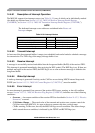
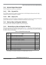
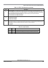
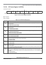
Table 15-3. IRSCI Transmit Pulse Width
TNP[1:0] Narrow Pulse Width
11 1/4
10 1/32
01 1/16
00 3/16
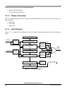
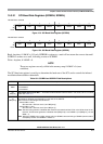
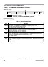
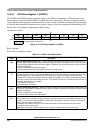
Module Base + 0x0002
76543210
R
LOOPS SCISWAI RSRC M WAKE ILT PE PT
W
Reset 00000000
Figure 15-5. SCI Control Register 1 (SCICR1)
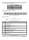
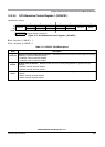
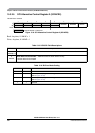
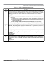
Table 15-4. SCICR1 Field Descriptions
Field Description
7
LOOPS
Loop Select Bit — LOOPS enables loop operation. In loop operation, the RXD pin is disconnected from the SCI
and the transmitter output is internally connected to the receiver input. Both the transmitter and the receiver must
be enabled to use the loop function.
0 Normal operation enabled
1 Loop operation enabled
The receiver input is determined by the RSRC bit.
6
SCISWAI
SCI Stop in Wait Mode Bit — SCISWAI disables the SCI in wait mode.
0 SCI enabled in wait mode
1 SCI disabled in wait mode
5
RSRC
Receiver Source Bit — When LOOPS = 1, the RSRC bit determines the source for the receiver shift register
input. See Table 15-5.
0 Receiver input internally connected to transmitter output
1 Receiver input connected externally to transmitter
4
M
Data Format Mode Bit — MODE determines whether data characters are eight or nine bits long.
0 One start bit, eight data bits, one stop bit
1 One start bit, nine data bits, one stop bit
3
WAKE
Wakeup Condition Bit — WAKE determines which condition wakes up the SCI: a logic 1 (address mark) in the
most significant bit position of a received data character or an idle condition on the RXD pin.
0 Idle line wakeup
1 Address mark wakeup